Fairchild Semiconductor 74F651SPC, 74F651SCX Datasheet

© 1999 Fairchild Semiconductor Corporation DS009581 www.fairchildsemi.com
March 1988
Revised August 1999
74F651 • 74F652 Transceivers/Registers
74F651 • 74F652
Transceivers/Registers
General Description
These devices consis t of bus transceiver circuits with Dtype flip-flops, and control circuitry arranged for multiplexed
transmission of data directly from the input bus or from
internal registers. Data on the A or B bus will be clocked
into the registers as the appropriate clock pin goes to HIGH
logic level. Output Enable pins (OEAB, OEBA
) are pro-
vided to control the transceiver function.
Features
■ Independent registers for A and B buses
■ Multiplexed real-time and stored data
■ Choice of non-inverting and inverting data paths
74F651 inverting
74F652 non-inverting
Ordering Code:
Devices also availab le in Tape and Reel. Specify by appending th e s uffix let t er “X” to the ordering code.
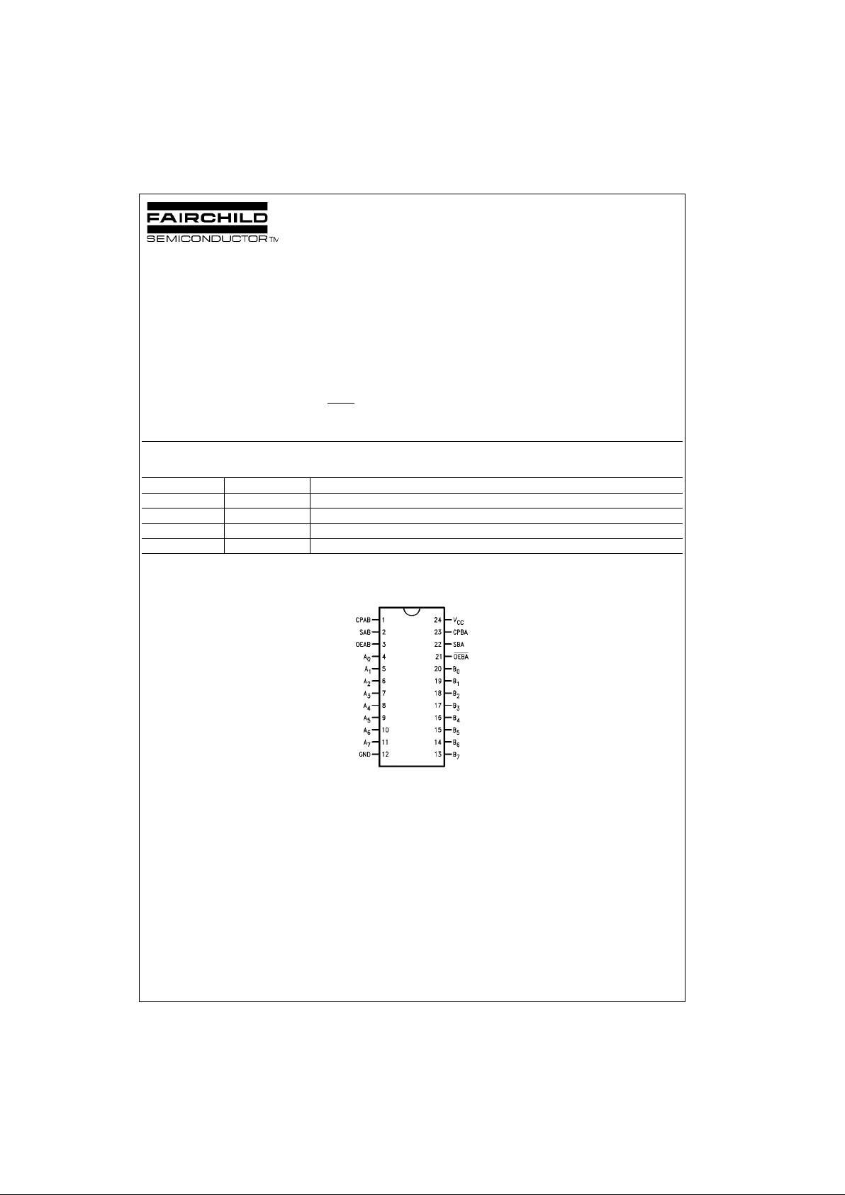
Connection Diagram
Order Number Package Number Package Description
74F651SC M24B 24-Lead Small Outline Integrated Circuit (SOIC), JEDEC MS-013, 0.300 Wide
74F651SPC N24C 24-Lead Plastic Dual-In-Line Package (PDIP), JEDEC MS-100, 0.300 Wide
74F652SC M24B 24-Lead Small Outline Integrated Circuit (SOIC), JEDEC MS-013, 0.300 Wide
74F652SPC N24C 24-Lead Plastic Dual-In-Line Package (PDIP), JEDEC MS-100, 0.300 Wide

www.fairchildsemi.com 2
74F651 • 74F652
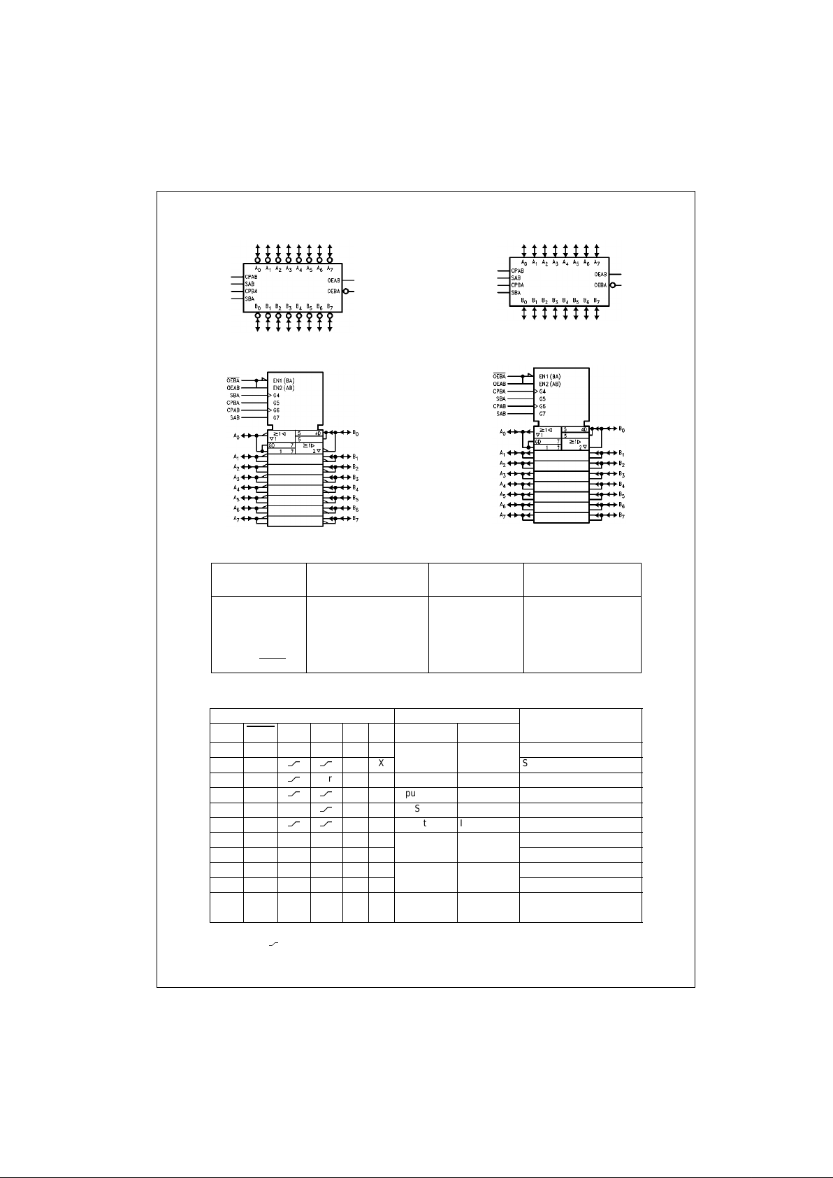
Logic Symbols
74F651
IEEE/IEC
74F651
74F652
IEEE/IEC
74F652
Unit Loading/Fan Out
Function Table
H = HIGH Voltage Level X = Immaterial
L = LOW Voltage Level
= LOW-to-HIGH Clock Transition
Note 1: The data output functions may be enabled or disabled by various signals at OEAB or OEBA inputs. Data input functions are always enabled,
i.e., data at the bus pins will be stored on eve ry LOW -t o-HIGH transition on th e c lock inputs.
Pin Names Description
U.L.
Input I
IH/IIL
HIGH/LOW
Output I
OH/IOL
A0–A7, B0–B
7
A and B Inputs/ 1.0/1.0 20 µA/−0.6 mA
3-STATE Outputs 600/106.6 (80) −12 mA/64 mA (48 mA)
CPAB, CPBA Clock Inputs 1.0/1.0 20 µA/−0.6 mA
SAB, SBA Select Inputs 1.0/1.0 20 µA/−0.6 mA
OEAB, OEBA
Output Enable Inputs 1.0/1.0 20 µA/−0.6 mA
Inputs Inputs/Outputs (Note 1)
Operating Mode
OEAB OEBA
CPAB CPBA SAB SBA
A
0
thru A7B0 thru B
7
L H H or L H or L X X Input Input Isolation
LH
X X Store A and B Data
XH
H or L X X Input Not Specified Store A, Hold B
HH
X X Input Output Store A in Both Registe rs
LXH or L
X X Not Specified Input Hold A, Store B
LL
X X Output Input Store B in Both Registers
L L X X X L Output Input Real-Time B Data to A Bus
L L X H or L X H Store B Data to A Bus
H H X X L X Input Output Real-Time A Data to B Bus
H H H or L X H X Stored A Data to B Bus
H L H or L H or L H H Output Output Stored A Data to B Bus and
Stored B Data to A Bus

3 www.fairchildsemi.com
74F651 • 74F652
Functional Description
In the transceiver mode , data present a t the HIGH impe dance port may be sto red in either the A or B register or
both.
The select (SAB, SBA) controls can multiplex stored and
real-time.
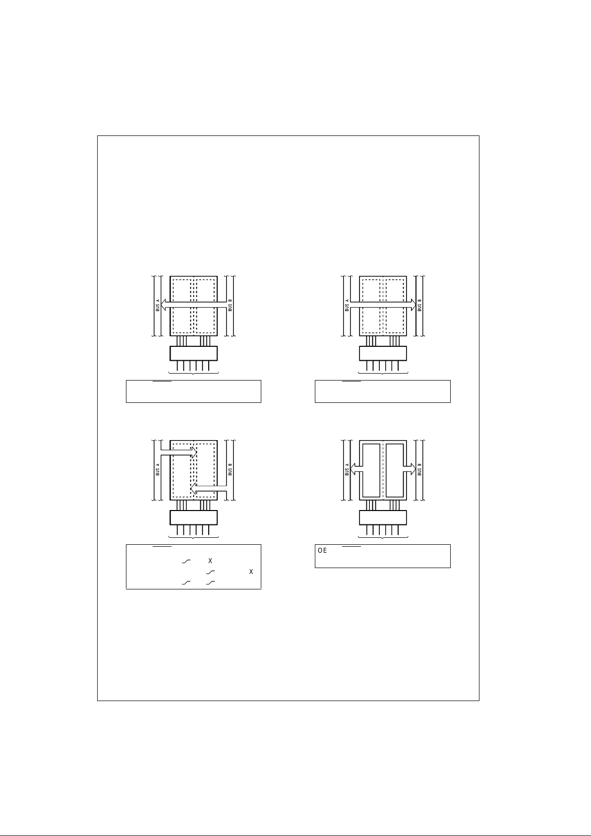
The examples in Figure 1 de monstr ate the fo ur funda mental bus-management func tions that can be perfor med with
the Octal bus transceivers and receivers.
Data on the A or B data bus, or both can be stored in the
internal D flip-flop by LOW-to-HIGH transitions at the
appropriate Clock Inp uts (CPAB, CPBA) regardless of the
Select or Output Enable Inputs. When SAB and SBA are in
the real time transfer m od e, it i s a lso po ssi ble to sto re d ata
without using the internal D flip-flops by simultaneously
enabling OEAB and OEBA. In this confi guration ea ch Output reinforces its Input. Thus when all other data sources to
the two sets of bus lines a re in a HIGH impedance state ,
each set of bus lines will remain at its last state.
Note A: Real-Time
Transfer Bus B to Bus A
Note B: Real-Time
Tran sfer Bus A to Bus B
Note C: Storage Note D: Transfer Storage
Data to A or B
FIGURE 1.
OEAB OEBA
CPAB CPBA SAB SBA
LLXXXL
OEAB OEBA CPAB CPBA SAB SBA
HHXXLX
OEAB OEBA CPAB CPBA SAB SBA
XH
XXX
LXX
XX
LH
XX
OEAB OEBA CPAB CPBA SAB SBA
H L H or L H or L H X
 Loading...