

Fairchild Semiconductor 74F648SPC, 74F648SCX, 74F648SC, 74F646BSPC, 74F646BSCX Datasheet
...
March 1988
Revised August 1999
74F646 • 74F646B • 74F648
Octal Transceiver/Register with 3-STATE Outputs
74F646 • 74F646B • 74F648 Octal Transceiver/ R egister with 3-STATE Outputs
General Description
These devices consist of bus transceive r circuits with 3STATE , D-type flip-fl ops, and c ontrol circui try arranged f or
multiplexed transmission of data directly from the input bus
or from the internal registers. Data on the A or B bus will be
clocked into the registers as the appropriate clock pin goes
to a high logic level. Control G
vided to control the tr ansceiver function. In the tran sceiver
mode, data present at the high impedance port may be
stored in either the A or the B register or in both. The select
controls can multiplex stored and real-time (transparent
mode) data. The direction control determines which bus
will receive data when the enable control G
In the isolation mode (control G
stored in the B register and/or B d ata ma y be store d in the
A register.
and direction pins are pr o-
is Active LOW.
HIGH), A data may be
Features
■ Independent registers for A and B buses
■ Multiplexed real-time and stored data
■ 74F648 has inverting data paths
■ 74F646/74F646B have non-inverting data paths
■ 74F646B is a faster version of the 74F646
■ 3-STATE outputs
■ 300 mil slim DIP
Ordering Code:
Order Number Package Number Package Description
74F646SC M24B 24-Lead Small Outline Integrated Circuit (SOIC), JEDEC MS-013, 0.300 Wide
74F646MSA MSA24 24-Lead Shrink Small Outline Package (SSOP), EIAJ TYPE II, 5.3mm Wide
74F646SPC N24C 24-Lead Plastic Dual-In-Line Package (PDIP), JEDEC MS-100, 0.300 Wide
74F646BSC M24B 24-Lead Small Outline Integrated Circuit (SOIC), JEDEC MS-013, 0.300 Wide
74F646BSPC N24C 24-Lead Plastic Dual-In-Line Package (PDIP), JEDEC MS-100, 0.300 Wide
74F648SC M24B 24-Lead Small Outline Integrated Circuit (SOIC), JEDEC MS-013, 0.300 Wide
74F648SPC N24C 24-Lead Plastic Dual-In-Line Package (PDIP), JEDEC MS-100, 0.300 Wide
Devices also availab le in Tape and Reel. Specify by appending th e s uffix let t er “X” to the ordering cod e.
© 1999 Fairchild Semiconductor Corporation DS009580 www.fairchildsemi.com
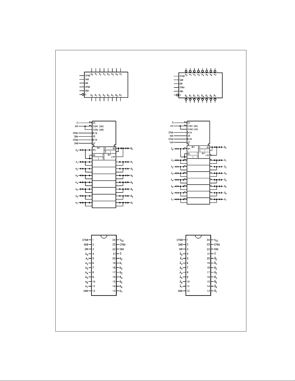
Logic Symbols
74F646 • 74F646B • 74F648
74F646/74F646B
IEEE/IEC
74F646/74F646B
74F648
IEEE/IEC
74F648
Connection Diagrams
74F646/74F646B 74F648
www.fairchildsemi.com 2
Unit Loading/Fan Out
Pin Names Description
A0–A
7
Data Register A Inputs/ 3.5/1.083 70 µA/−650 µA
3-STATE Outputs 600/106.6 (80) −12 mA/64 mA (4 8 mA)
B
0–B7
Data Register B Inputs/ 3.5/1.083 70 µA/−650 µA
3-STATE Outputs 600/106.6 (80) −12 mA/64 mA (4 8 mA)
CPAB, CPBA Clock Pulse Inputs 1.0/1.0 20 µA/−0.6 mA
SAB, SBA Select Inputs 1.0/1.0 20 µA/−0.6 mA
G
Output Enable Input 1.0/1.0 20 µA/−0.6 mA
DIR Direction Control Input 1.0/1.0 20 µA/−0.6 mA
U.L.
HIGH/LOW
Output I
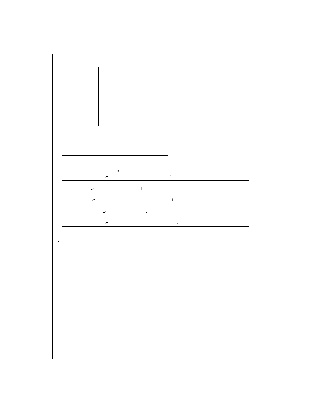
Function Table
Input I
74F646 • 74F646B • 74F648
IH/IIL
OH/IOL
Inputs Data I/O (Note 1)
DIR CPAB CPBA SAB SBA
G
A
0–A7B0–B7
Function
H X H or L H or L X X Isolation
HX
HXX
LHXXLX A
LH
L H H or L X H X A Register to B
LH
X X X Input Input Clock An Data into A Register
X X Clock Bn Data into B Register
to Bn—Real Time (Transparent Mode)
X L X Input Output Clock An Data into A Register
X H X Clock An Data into A Register and Output to B
n
(Stored Mode)
n
LLXXXL Bn to An—Real Time (Transparent Mode)
LLX
L L X H or L X H B Register to A
LLX
H = HIGH Voltage Level
L = LOW Voltage Level
X = Irrelevant
= LOW-to - HIGH Transition
Note 1: The data output functions may be enabled or disabled by various signals at the G
at the bus pins will be stored on every LOW-to-HIGH transition of the clo c k in puts.
X L Output Input Clock Bn Data into B Register
(Stored Mode)
X H Clock Bn Data into B Register and Output to A
and DIR Inputs. Data input functions are always enabled; i.e ., d at a
n
n
n
3 www.fairchildsemi.com
 Loading...