Fairchild Semiconductor 74F579PC, 74F579SJ, 74F579SCX, 74F579SC Datasheet

© 1999 Fairchild Semiconductor Corporation DS009568 www.fairchildsemi.com
April 1988
Revised August 1999
74F579 8-Bit Bidirectional Binary Counter with 3-STATE Outputs
74F579
8-Bit Bidirectional Binary Counter with 3-STATE Outputs
General Description
The 74F579 is a fully synchronous 8-stage up/down
counter with multiplexed 3-STATE I/O ports for bus-oriented applications. It featur es a preset capability for programmable operation , carry loo kahead for easy cascad ing
and a U/D
input to control the direction of counting. All state
changes, whether in coun ting or parallel loading , are initiated by th e rising edge of the clock.
Features
■ Multiplexed 3-STATE I/O ports
■ Built-in lookahead carry capability
■ Count frequency 100 MHz typical
■ Supply current 75 mA typical
■ Guarante ed 4000V minimum ESD protection
Ordering Code:
Devices also availab le in Tape and Reel. Specify by appending th e s uffix let t er “X” tot he ordering code.
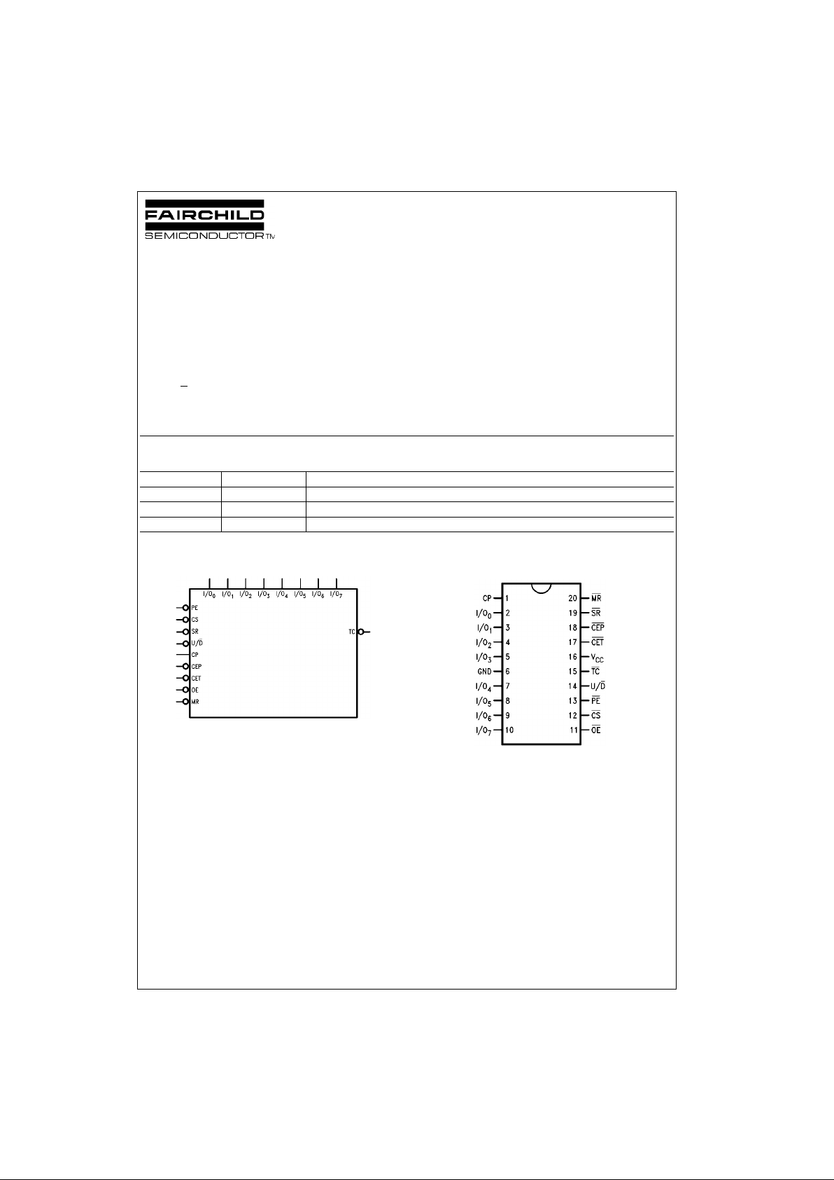
Logic Symbol Connection Diagram
Order Number Package Number Package Description
74F579SC M20B 20-Lead Small Outline Integrated Circuit (SOIC), JEDEC MS-013, 0.300 Wide
74F579SJ M20D 20-Lead Small Outline Package (SOP), EIAJ TYPE II, 5.3mm Wide
74F579PC N20A 20-Lead Plastic Dual-In-Line Package (PDIP), JEDEC MS-001, 0.300 Wide

www.fairchildsemi.com 2
74F579
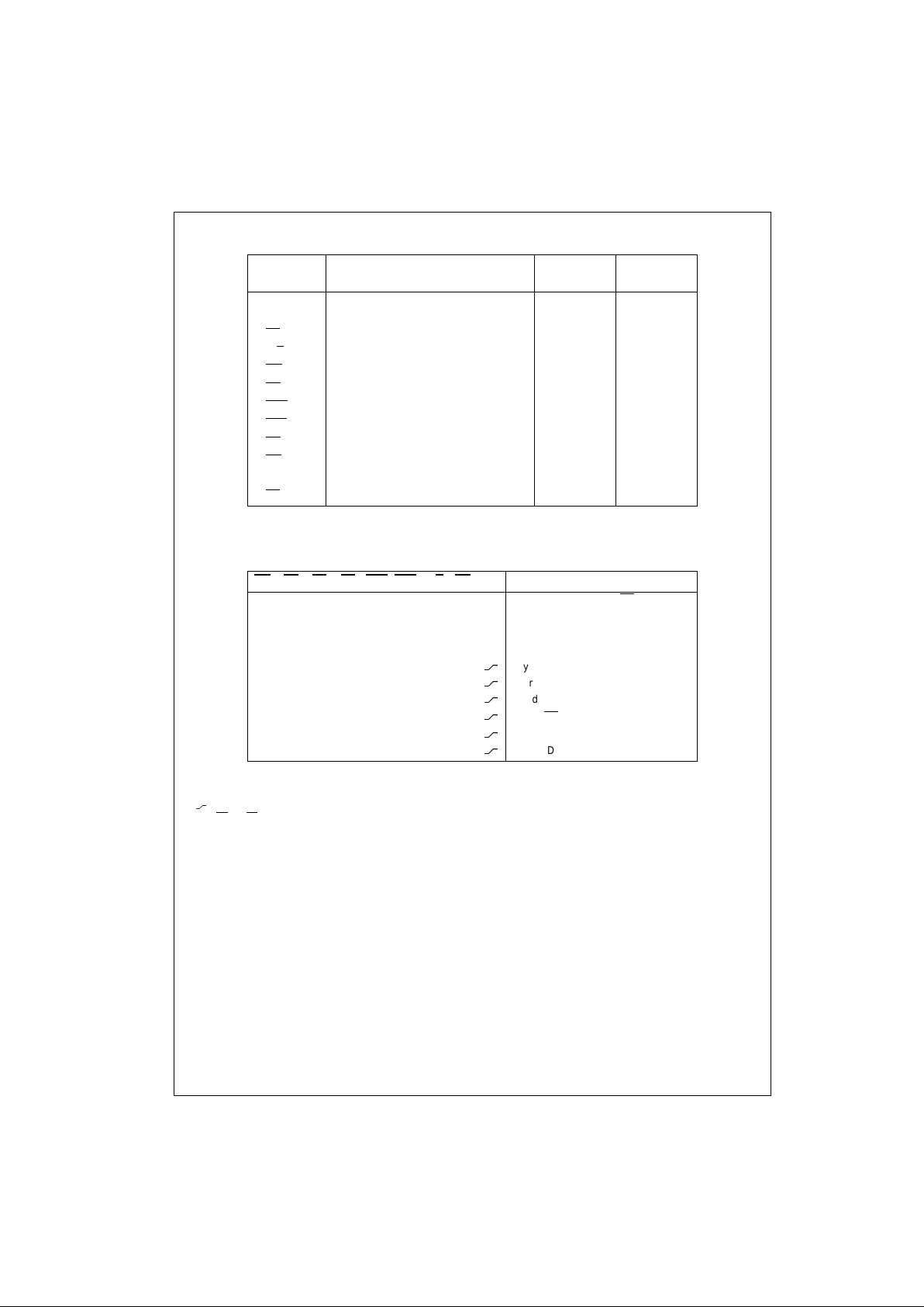
Unit Loading/Fan Out
Function Table
H = HIGH Voltage Level
L = LOW Voltage Level
X = Immaterial
= LOW to HIGH Clock Transition
Not LL = CS
and PE should never both be LOW voltage level at the same time.
Pin Names Description
U.L.
Input I
IH/IIL
HIGH/LOW
Output I
OH/IOL
I/O0–I/O
7
Data Inputs or 3.5/0.333 70 µA/−0.2 mA
3-STATE Outputs 75/15 −3 mA/24 mA
PE
Parallel Enable Input (Active LOW) 0.25/0.333 5 µA/−0.2 mA
U/D
Up-Down Count Control Input 0.25/0.333 5 µA/−0.2 mA
MR
Master Reset Input (Active LOW) 0.25/0.333 5 µA/−0.2 mA
SR
Synchronous Reset Input (Active LOW) 0.25/0.333 5 µA/−0.2 mA
CEP
Count Enable Parallel Input (Active LOW) 0.25/0.333 5 µA/−0.2 mA
CET
Count Enable Trickle Input (Active LOW) 0.25/0.333 5 µA/−0.2 mA
CS
Chip Select Input Active (Active LOW) 0.25/0.333 5 µA/−0.2 mA
OE
Output Enable Input (Active LOW) 0.25/0.333 5 µA/−0.2 mA
CP Clock Pulse Input (Active Rising Edge) 0.25/0.333 5 µA/−0.2 mA
TC
Terminal Count Output (Active LOW) 25/12.5 −1 mA/5 mA
MR SR CS PE CEP CET U/D OE CP Function
XXHXXXXXXI/O
a
to I/Oh in High Z (PE Disabled)
XXLHXXXHXI/O
a
to I/Oh in High Z
X X L H X X X L X Flip-Flop Outputs Appear on I/O Lines
L X X X X X X X X Asynchronous Reset for all Flip-Flops
HLXXXXXX
Synchronous Reset for all Flip-Flops
HHLLXXXX
Parallel Load all Flip-Flops
H H (Not LL) H X X X
Hold
H H (Not LL) X H X X
Hold (TC Held HIGH)
H H (Not LL) L L H X
Count Up
H H (Not LL) L L L X
Count Down

3 www.fairchildsemi.com
74F579
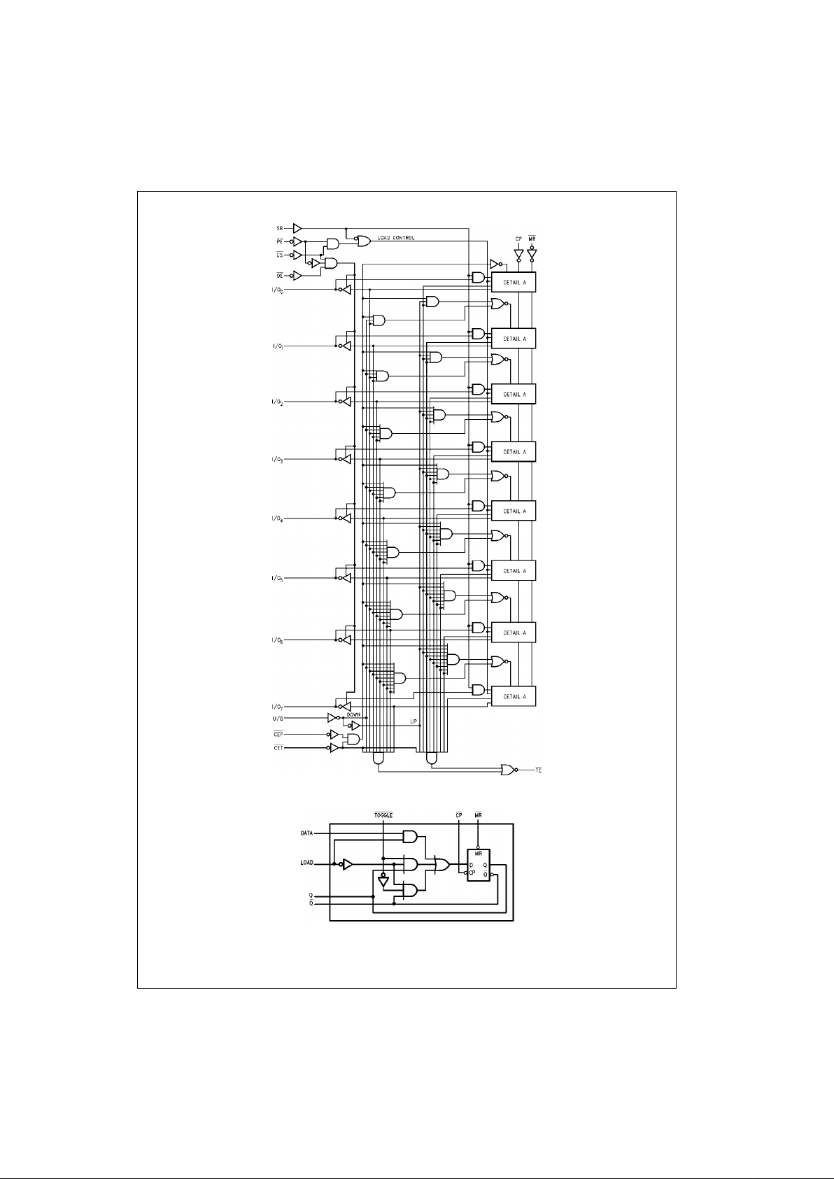
Logic Diagrams
Please note that this d iagram is provided only f or t he understanding of lo gic operations and should not be used to estimat e propagation delays.
V
CC
= Pin 16 GND = Pin 6 () = Pin Numbers
Detail A
 Loading...