Fairchild Semiconductor 74F569SJ, 74F569SCX, 74F569SC, 74F569PC Datasheet

© 1999 Fairchild Semiconductor Corporation DS009565 www.fairchildsemi.com
April 1988
Revised August 1999
74F569 4-Bit Bidirectional Counter with 3-STATE Outputs
74F569
4-Bit Bidirectional Counter with 3-STATE Outputs
General Description
The 74F569 is a ful ly synchro nou s, rever sible c ounter with
3-STATE ou tputs. The 74F569 is a binary coun ter, featuring preset capability for programmable operation, carry lookahead for easy c ascading, a nd a U/D
input to control the
direction of counting. For maximum flexibility there are both
synchronous and master asynchronous reset inputs as well
as both Clocked Carry (CC
) and Terminal Count (TC) outputs. All state changes except Master Reset are initiated by
the rising edge of the clock. A HIGH signal on the Output
Enable (OE
) input forces the output buffers into the high
impedance state but does not prevent counti ng, resetting
or parallel loading.
Features
■ Synchronous counting and loading
■ Lookahead carry capability for easy cascading
■ Preset capability for programmable operation
■ 3-STATE outputs for bus organized systems
Ordering Code:
Devices also availab le in Tape and Reel. Specify by appending th e s uffix let t er “X” to the ordering code.
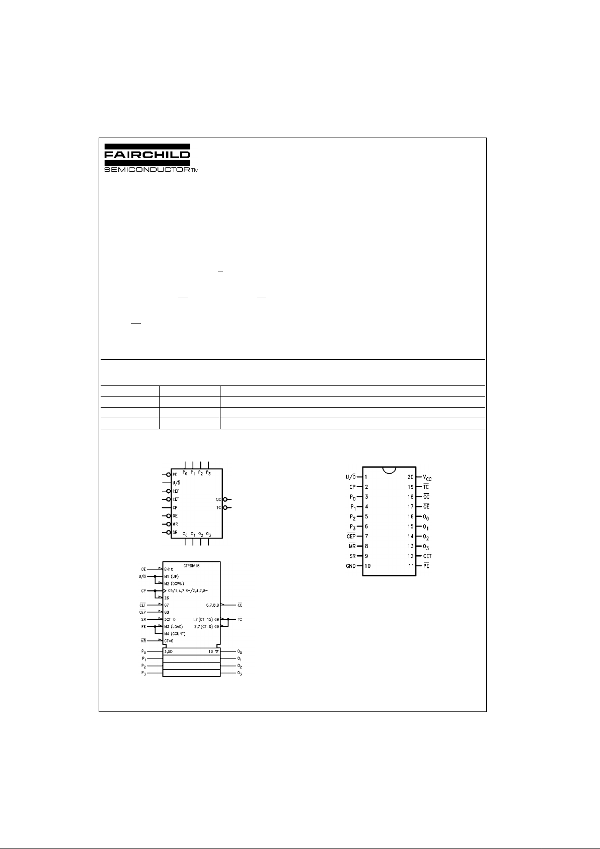
Logic Symbols
IEEE/IEC
Connection Diagram
FAST is a regist ered trademark of Fairc hild Semiconductor C orporation.
Order Number Package Number Package Description
74F569SC M20B 20-Lead Small Outline Integrated Circuit (SOIC), JEDEC MS-013, 0.300 Wide
74F569SJ M20D 20-Lead Small Outline Package (SOP), EIAJ TYPE II, 5.3mm Wide
74F569PC N20A 20-Lead Plastic Dual-In-Line Package (PDIP), JEDEC MS-001, 0.300 Wide

www.fairchildsemi.com 2
74F569
Unit Loading/Fan Out
Functional Description
The 74F569 counts in the modulo-16 binary sequence.
From state 15 it will increment to state 0 in the Up mode; in
the Down mode it will decrement from 0 to 15. The clock
inputs of all flip-flops a re driven in para llel through a clock
buffer. All state changes (except due to Master Reset)
occurs synchronously with the LOW-to-HIGH trans ition of
the Clock Pulse (CP) input signal.
The circuits have five fundamental mo des of operation, in
order of precedence: asynchronous reset, synchronous
reset, parallel load, count an d hold. Five control inputs—
Master Reset (MR
), Synchronous Reset (SR), Parallel
Enable (PE
), Count Enable Parallel (CEP) and Count
Enable Trickle CET
)—plus the Up/Down (U/D) input, determine the mode of operation , as shown in the Mod e Select
Table. A LOW signal on MR
overrides all other i nputs and
asynchronously forces the flip-flop Q outputs LOW. A LOW
signal on SR
overrides counti ng and parallel loading and
allows the Q outpu ts to g o LOW on the n ext risi ng ed ge of
CP. A LOW signal on PE
overrides counting and a llows
information on the Parallel Data (P
n
) inputs to be lo aded
into the flip-flops on the next rising edge of CP. With MR
,
SR
and PE HIGH, CEP and CET permit counting when
both are LOW. Conversely, a HIGH signal on either CEP
or
CET
inhibits counting.
The 74F569 uses edge-triggered flip-flops and changing
the SR
, PE, CEP, CET or U/D inputs when the CP is in
either state does not cause errors, provided that the recommended setup and hold times, with respect to the rising
edge of CP, are observed.
Two types of outputs are pro vided as overflow/underflow
indicators. The Terminal Count (TC
) output is normally
HIGH and goes LOW providing CET
is LOW, when the
counter reaches zero in th e Down m ode, o r rea ches ma ximum
(15) in the Up mode. TC
will then remain LOW until a state
change occurs, whethe r by counting or prese tting, or until
U/D
or CET is changed. To implement synchronous multi-
stage counters, the connections between the TC
output
and the CEP
and CET inputs can provide either slow or
fast carry propagation.
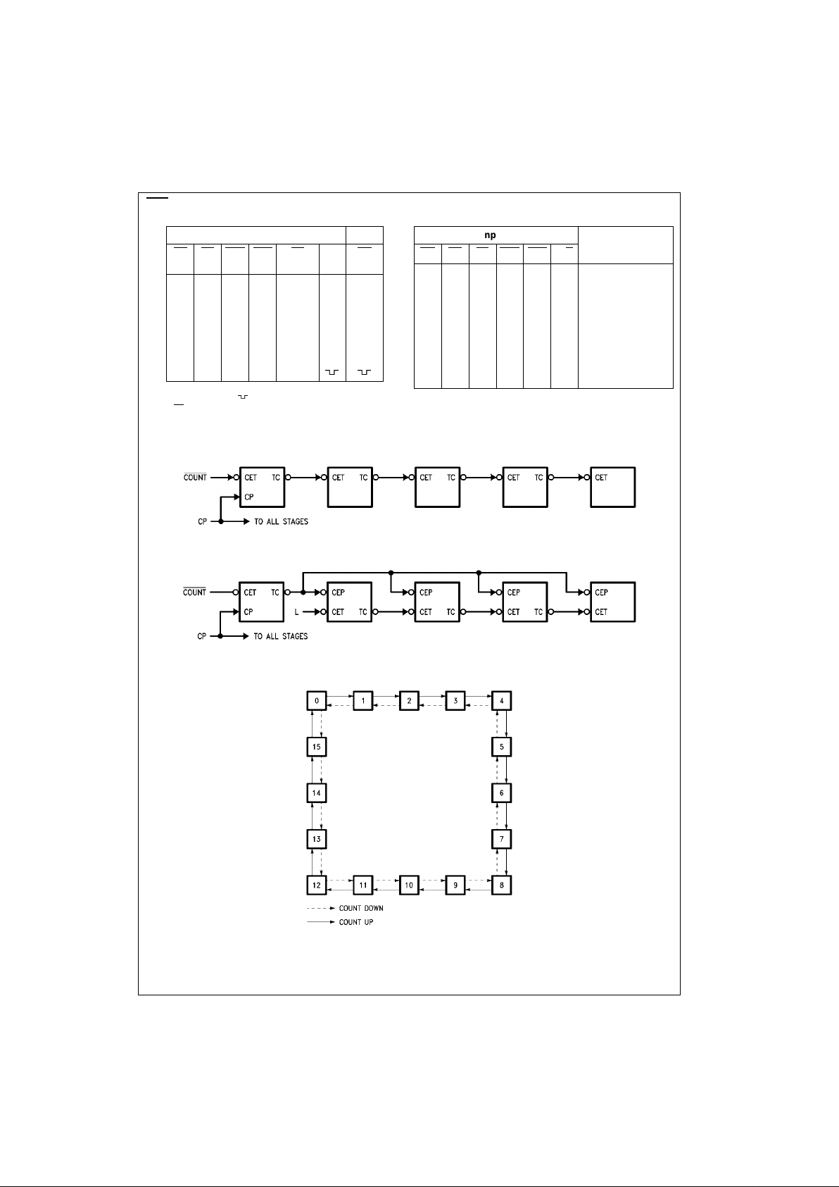
Figure 1 shows the connections for simple ripple carry, in
which the clock period must be longer than the CP to TC
delay of the first stage, plus the cumulative CET to TC
delays of the intermediate stages, plus the CET to CP
setup time of the last stage. This total delay plus setup time
sets the upper limit o n clock frequency. For faster clock
rates, the carry lookahead connecti ons shown in Figure 2
are recommended. In this sch eme the ripple del ay through
the intermediate stages commences with the same clock
that causes the first stage to tick over from m ax to min in
the Up mode, or m in to m ax in th e Dow n mo de, to start its
final cycle. Since this final cycle takes 16 clocks to complete, there is plenty of time for the ripple to progress
through the intermediate stages. The critical timing that limits the clock period is th e CP to TC
delay of the first stage
plus the CEP
to CP setup time of the last stage. The TC
output is subject t o decoding spikes due to intern al race
conditions and is th erefore not recommen ded for u se as a
clock or asynchronous reset for flip-flops, registers or
counters. For such applications, the Clocke d Carry (CC
)
output is provided. The CC
output is normally HIGH. Wh en
CEP
, CET, and TC are LOW, the CC output will go LO W
when the clock next goes LOW and will stay LOW until the
clock goes HIGH again, as shown in the CC
Truth Ta ble.
When the Output Enable (OE
) is LOW, the parallel data
outputs O
0–O3
are active and follow the flip-flop Q outputs.
A HIGH signal on OE
forces O0–O3 to the High Z state but
does not prevent counting, loading or resetting.
Logic Equations
Count Enable = CEP • CET • PE
Up: TC
= Q0 • Q1 • Q2 • Q3 • (Up) • CET
Down: TC = Q0 • Q1 • Q2 • Q3 • (Down) • CET
Pin Names Description
U.L.
Input I
IH/IIL
HIGH/LOW
Output I
OH/IOL
P0–P
3
Parallel Data Inputs 1.0/1.0 20 µA/−0.6 mA
CEP
Count Enable Parallel Input (Active LOW) 1.0/1.0 20 µA/−0.6 mA
CET
Count Enable Trickle Input (Active LOW) 1.0/1.0 20 µA/−1.2 mA
CP Clock Pulse Input (Active Rising Edge) 1.0/1.0 20 µA/−0.6 mA
PE
Parallel Enable Input (Active LOW) 1.0/1.0 20 µA/−1.2 mA
U/D
Up/Down Count Control Input 1.0/1.0 20 µA/−0.6 mA
OE
Output Enable Input (Active LOW) 1.0/1.0 20 µA/−0.6 mA
MR
Master Reset Input (Active LOW) 1.0/1.0 20 µA/−0.6 mA
SR
Synchronous Reset Input (Active LOW) 1.0/1.0 20 µA/−0.6 mA
O
0–O3
3-STATE Parallel Data Outputs 150/40(33.3) −3 mA/24 mA (20 mA)
TC
Terminal Count Output (Active LOW) 50/33.3 −1 mA/20 mA
CC
Clocked Carry Output (Active LOW) 50/33.3 −1 mA/20 mA

3 www.fairchildsemi.com
74F569
CC Truth Table
H = HIGH Voltage Level X = Immaterial
L = LOW Voltage Level
= HIGH-to-LOW-to- H IG H C lock Transition
Note 1: TC
is generated internally
Mode Select Table
H = HIGH Voltage Level
L = LOW Voltage Level
X = Immaterial
FIGURE 1. Multistage Counter with Ripple Carry
FIGURE 2. Multistage Counter with Lookahead Carry
State Diagram
Inputs Output
SR
PE CEP CET TC
(Note 1)
CP CC
LXXX X X H
XLXX X X H
XXHX X X H
XXXH X X H
XXXX H X H
HHL L L
Inputs Operating
MR
SR PE CEP CET U/D Mode
L X X X X X Asynchronous Reset
H L X X X X Synchronous Reset
H H L X X X Parallel Load
HHHHXXHold
H H H X H X Hold
H H H L L H Count Up
H H H L L L Count Down
 Loading...