Fairchild Semiconductor 74F552SCX, 74F552SC, 74F552QC Datasheet

© 2000 Fairchild Semiconductor Corporation DS009561 www.fairchildsemi.com
April 1988
Revised March 2000
74F552 Octal Registered Transceiver with Parity and Flags
74F552
Octal Registered Transceiver with Parity and Flags
General Description
The 74F552 octal transc eiver contains two 8-bit regi sters
for temporary storage of data flowing in either direction.
Each register has its own clock pulse and clock enable
input as well as a flag flip-flop that is set automat ically as
the register is loaded. The flag output will be reset when
the output enable returns to HIGH af ter reading the output
port. Each register has a separate output enable control for
its 3-STATE buffer. The separate Clocks, Flags, and
Enables provide considerable flexibility as I/O ports for
demand-response data transfer. When data is tra nsferred
from the A Port to the B Po rt, a parity b it is generat ed. On
the other hand, when da ta i s tr ansf err ed from the B Port to
the A Port, the parity of input data on B
0–B7
is checked.
Features
■ 8-Bit bidirectional I/O Port with handshake
■ Register status flag flip-flops
■ Separate clock enable and output enable
■ Parity generation and parity check
■ B-outputs sink 64 mA
■ 3-STATE outputs
Ordering Code:
Devices also availab le in Tape and Reel. Specify by appending th e s uffix let t er “X” to the ordering code.
Connection Diagrams
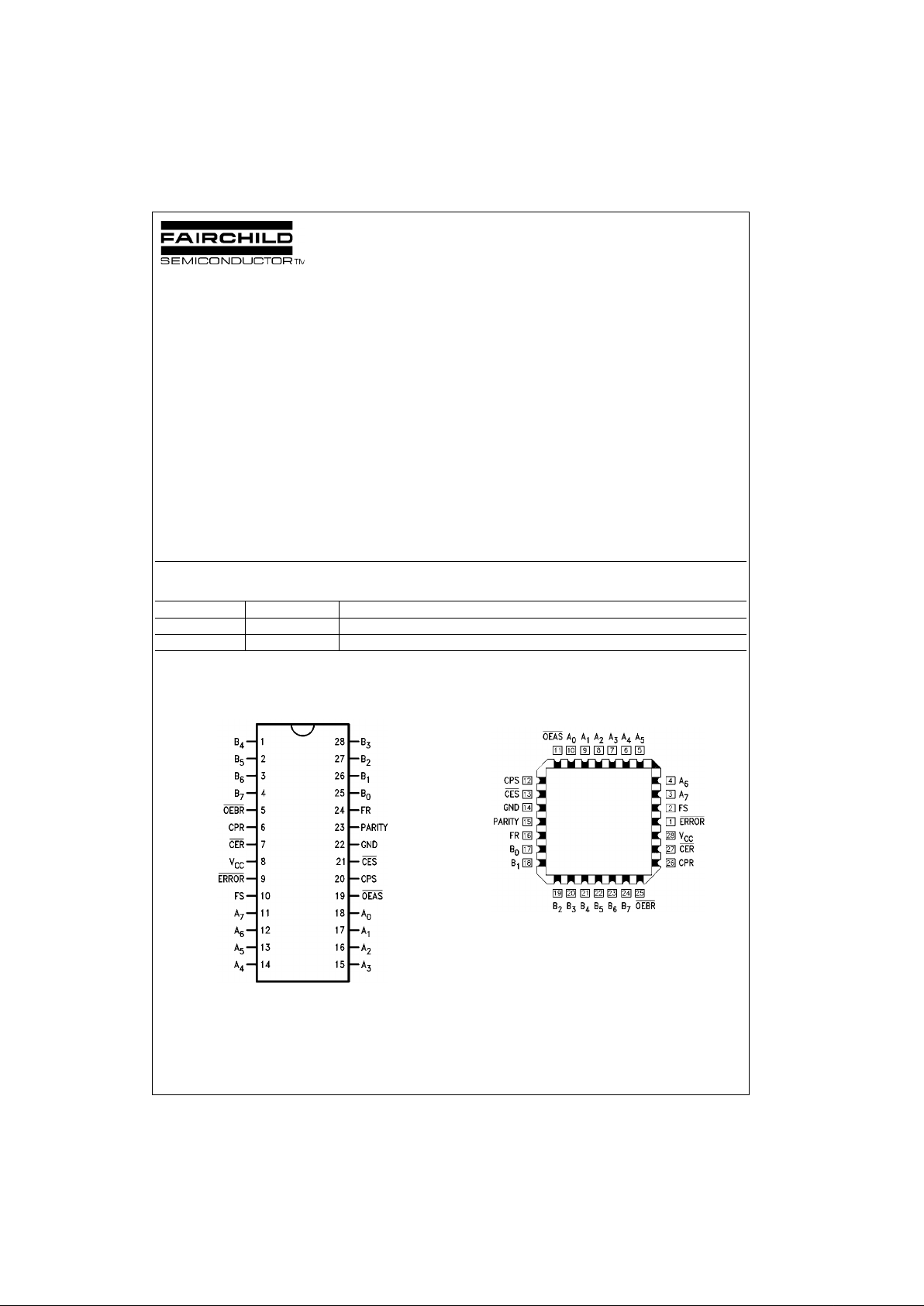
Pin Assignments for SOIC Pin Assignments for PLCC
Order Number Package Number Package Description
74F552SC M28B 28-Lead Small Outline Integrated Circuit (SOIC), JEDEC MS-013, 0.300 Wide
74F552QC V28A 28-Lead Plastic Lead Chip Carrier (PLCC), JEDEC MO-047, 0.450 Square

www.fairchildsemi.com 2
74F552
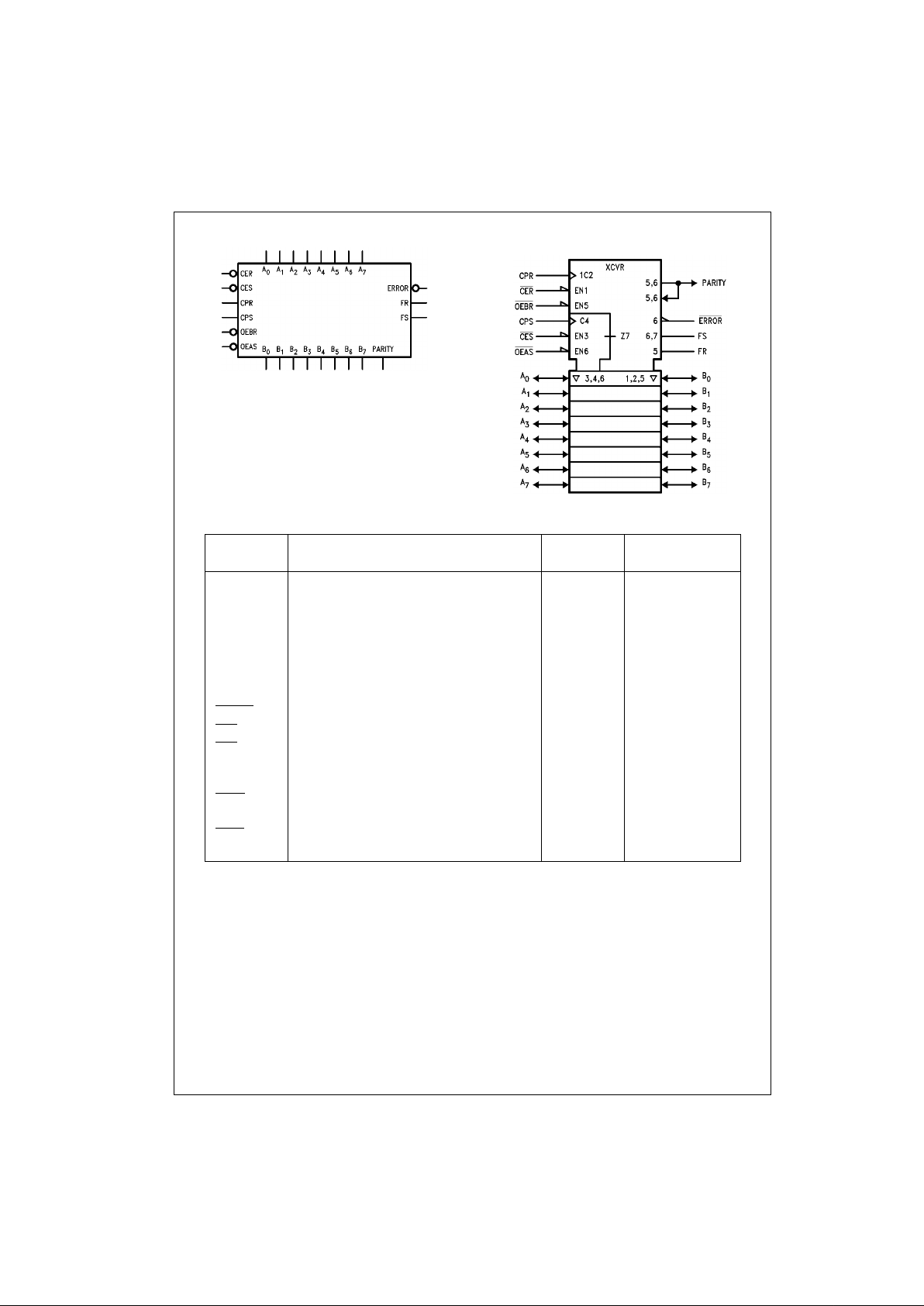
Logic Symbols
IEEE/IEC
Unit Loading/Fan Out
Pin Names Description
U.L.
Input I
IH/IIL
HIGH/LOW
Output I
OH/IOL
A0–A
7
A-to-B Port Data Inputs or 3.5/1.083 70 µA/−0.65 mA
B-to-A 3-STATE 150/40 (33.3) −3 mA/24 mA (20 mA)
B
0–B7
B-to-A Transceiver Inputs or 3.5/1.083 70 µA/−0.65 mA
A-to-B 3-STATE Output 600/106.6 (80) −12 mA/64 mA (48 mA)
FR B Port Flag Output 50/33.3 −1 mA/20 mA
FS A Port Flag Output 50/33.3 −1 mA/20 mA
PARITY Parity Bit Transceiver Input or Output 3.5/1.083 70 µA/−0.65 mA
600/106.6 ( 50) −12 mA/64 mA (48 mA)
ERROR
Parity Check Output (Active LOW) 50/33.3 −1 mA/20 mA
CER
R Registers Clock Enable Input (Active LOW) 1.0/1.0 20 µA/−0.6 mA
CES
S Registers Clock Enable Input (Active LOW) 1.0/1.0 20 µA/−0.6 mA
CPR R Registers Clock Pulse Input (Active Rising Edge) 1.0/1.0 20 µA/−0.6 mA
CPS S Registers Clock Pulse Input (Active Rising Edge) 1.0/1.0 20 µA/−0.6 mA
OEBR
B Port and PARITY Output Enable (Active LOW) 1.0/2.0 20 µA/−1.2 mA
and Clear FR Input (Active Rising Edge)
OEAS
A Port Output Enable (Active LOW) 1.0/2.0 20 µA/−1.2 mA
and Clear FS Input (Active Rising Edge)

3 www.fairchildsemi.com
74F552
Functional Description
Data applied to the A-inputs are entered and stored in the
R register on the rising edge of the CPR Clock Puls e, provided that the Clock Enable (CER
) is LOW; simultaneously,
the status flip-flop is set and the flag (FR) output goes
HIGH. As the Clock Enable (CER
) returns to HIGH, the
data will be held in the R regi ster. These data ent ere d fro m
the A-inputs will appear at the B Port I/O pins after the Output Enable (OEBR
) has gone LOW. When OEBR is LOW,
a parity bit appears at the PARITY pin, which will be set
HIGH when th er e is a n e v en nu m be r of 1s or a ll 0s at t h e Q
outputs of the R register. After the data i s assimilated, t he
receiving system clears the flag FR by ch anging the sig nal
at the OEBR
pin from LOW-to-HIGH.
Data flow from B-to-A proceeds in the same manner
described for A-to-B flow. A LOW at the CES
pin and a
LOW-to-HIGH transition at CPS pin enters the B-input data
and the parity-input da ta into th e S re gisters a nd the p arity
register respectively and set the f lag o utput FS to HIGH . A
LOW signal at the OEAS
pin enables the A Port I/O pins
and a LOW-to-HIGH t ransition of the OEAS
signal clears
the FS flag. When OEAS
is LOW, the parity check outpu t
ERROR
will be HIGH if there is an odd number of 1s at the
Q outputs of the S registers and the parity register. The flag
FS can be cleared by a LOW-to-HIGH transition of the
OEAS
signal.
Register Function Table
(Applies to R or S Register)
H = HIGH Voltage Level
= LOW-to - HIGH Transition
L = LOW Voltage Level † = Not LOW-to-HIGH Transition
X = Immaterial NC = No Change
Output Control
H = HIGH Voltage Level X = Immaterial
L = LOW Voltage Level Z = High Impeda nc e
Flag Flip-Flop Function Table
(Applies to R or S Flag Flip-Flop)
H = HIGH Voltage Level
= LOW-to-HIGH Transition
L = LOW Voltage Level † = Not LOW-to-HIGH Transition
X = Immaterial NC = No Change
Parity Generation Function
H = HIGH Voltage Level X = Immaterial
L = LOW Voltage Level Z = High Impedance
Parity Check Function
H = HIGH Voltage Level
L = LOW Voltage Level
X = Immaterial
Inputs Internal
Function
DCPCE
Q
XXH NCHold Data
L
LL
Load Data
H
LH
X † L NC Keep Old Data
OE
Internal A or B
Function
Q Outputs
H X Z Disable Output
L L L Enable Output
L H H Enable Output
Inputs Flag
Function
CE
CP OE Output
H X † NC Hold Flag
L
†HSet Flag
XX
L Clear Flag
OEBR
Number of HIGHs in the
Parity Output
Q Outputs of the R Register
HX Z
L 0, 2, 4, 6, 8 H
L 1, 3, 5, 7 L
OEAS
Number of HIGHs in Parity ERROR
the Q Outputs of the S Register Input Output
HXXH
L 0, 2, 4, 6, 8 L L
L 1, 3, 5, 7 L H
L 0, 2, 4, 6, 8 H H
L 1, 3, 5, 7 H L
 Loading...