Fairchild Semiconductor 74F540SJ, 74F540SCX, 74F540SC, 74F540PC Datasheet

© 1999 Fairchild Semiconductor Corporation DS009553 www.fairchildsemi.com
April 1988
Revised August 1999
74F540 • 74F541 Octal Buffer/Line Driver with 3-STATE Outputs
74F540 • 74F541
Octal Buffer/Line Driver with 3-STATE Outputs
General Description
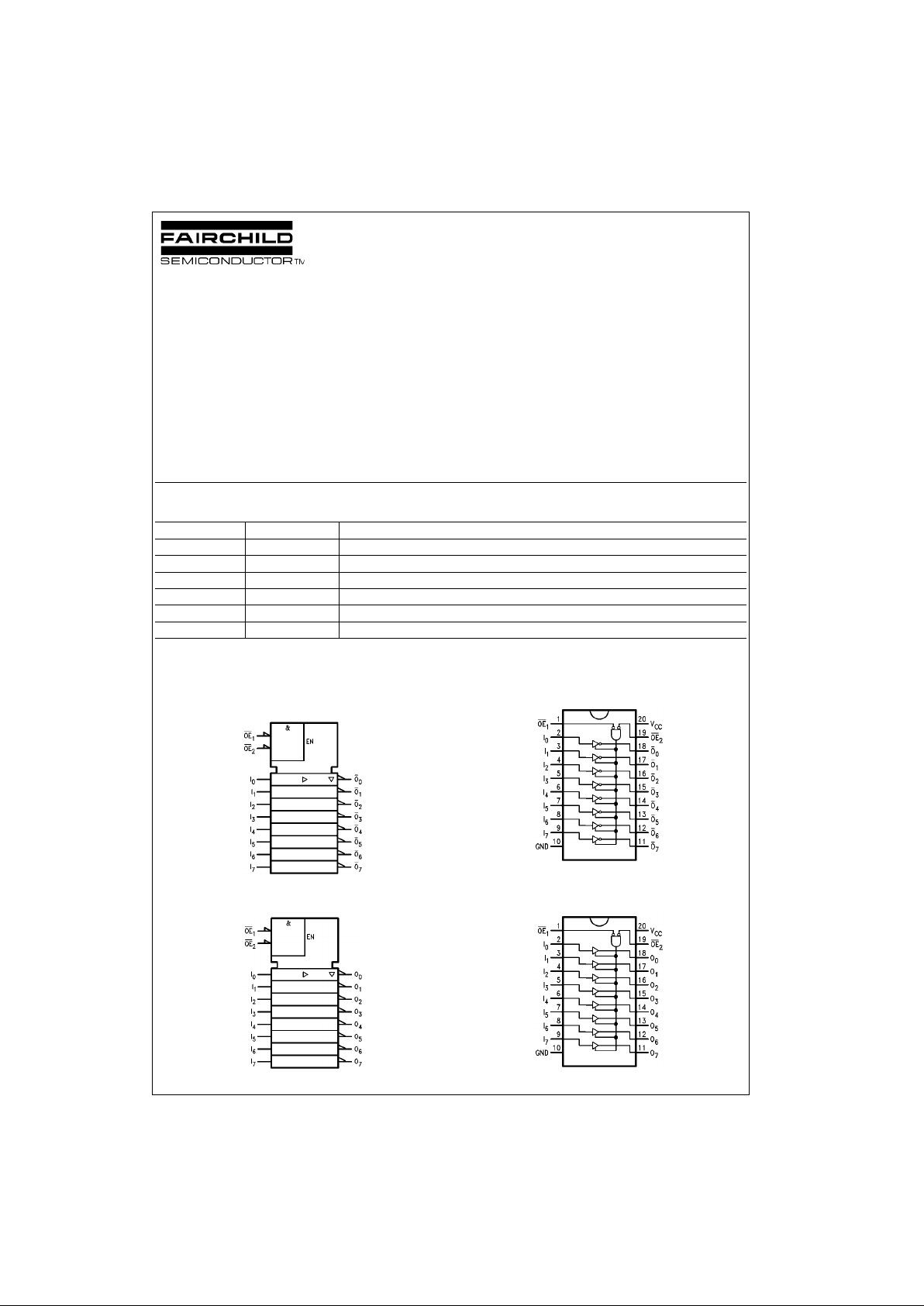
The 74F540 and 74F541 are similar in function to the
74F240 and 74F244 respectively, except that the inputs
and outputs are on opposite sides of the package (see
Connection Diagrams). This pinout arrangement makes
these devices especially use ful as output ports for micr oprocessors, allowing ease of layou t and grea ter PC board
density.
Features
■ 3-STATE outputs drive bus lines
■ Inputs and outputs opposite side of package, allowing
easier interface to microprocessors
Ordering Code:
Devices also availab le in Tape and Reel. Specify by appending th e s uffix let t er “X” to the ordering code.
Logic Symbols
IEEE/IEC
74F540
IEEE/IEC
74F541
Connection Diagrams
74F540
74F541
Order Number Package Number Package Description
74F540SC M20B 20-Lead Small Outline Integrated Circuit (SOIC), JEDEC MS-013, 0.300 Wide
74F540SJ M20D 20-Lead Small Outline Package (SOP), EIAJ TYPE II, 5.3mm Wide
74F540PC N20A 20-Lead Plastic Dual-In-Line Package (PDIP), JEDEC MS-001, 0.300 Wide
74F541SC M20B 20-Lead Small Outline Integrated Circuit (SOIC), JEDEC MS-013, 0.300 Wide
74F541SJ M20D 20-Lead Small Outline Package (SOP), EIAJ TYPE II, 5.3mm Wide
74F541PC N20A 20-Lead Plastic Dual-In-Line Package (PDIP), JEDEC MS-001, 0.300 Wide

www.fairchildsemi.com 2
74F540 • 74F541
Unit Loading/Fan Out
Truth Table
H = HIGH Voltage Level
L = LOW Voltage Level
X = Immaterial
Z = High Impedance
Pin Names Description
U.L.
Input I
IH/IIL
HIGH/LOW
Output I
OH/IOL
OE1, OE
2
3-STATE Output Enable Input (Active LOW) 1.0/1.0 20 µA/−0.6 mA
I
n
Inputs 1.0/1.0 20 µA/−0.6 mA
O
n
, O
n
Outputs 600/106.6 (80) −12 mA/64 mA (48 mA)
Inputs Outputs
OE
1
OE
2
I 74F540 74F541
LLHLH
HXXZZ
XHXZZ
LLLHL
 Loading...