

Fairchild Semiconductor 74F539SCX, 74F539SC, 74F539PC, 74F539CW Datasheet
© 1999 Fairchild Semiconductor Corporation DS009552 www.fairchildsemi.com
April 1988
Revised August 1999
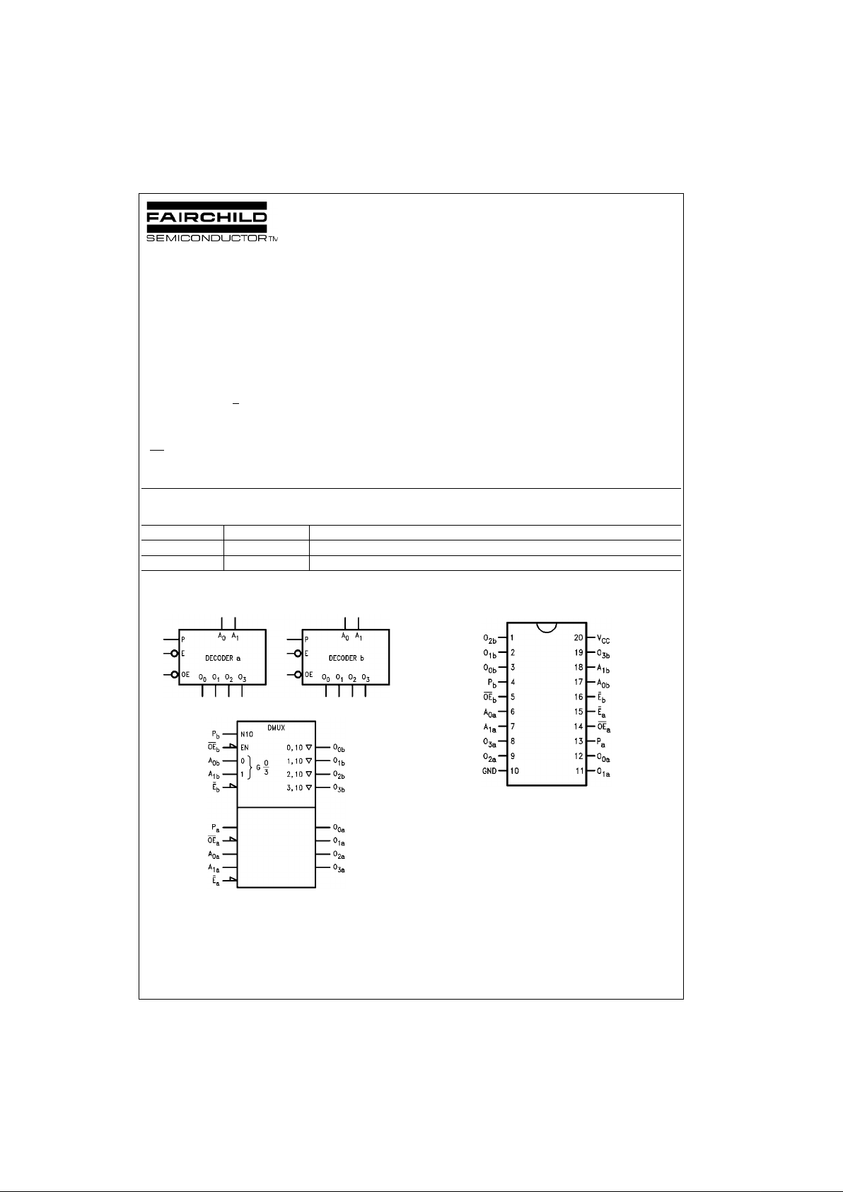
74F539 Dual 1-of-4 Decoder with 3-STATE Outputs
74F539
Dual 1-of-4 Decoder with 3-STATE Outputs
General Description
The 74F539 contains two independent decoders. Each
accepts two Address (A
0
, A1) input signals and d ecodes
them to select one of four mutually exclu sive outputs. A
polarity control in put (P) determines whether the o utputs
are active HIGH (P = L) or active LOW (P = H). An active
LOW input Enable (E
) is available for data demultiplexing;
data is routed to the selected output in non-inverted form in
the active LOW mode or in inverted form in the active HIGH
mode. A HIGH signal on the acti ve LOW Output Enable
(OE
) input forces the 3-STATE outputs to the high imped-
ance state.
Ordering Code:
Devices also availab le in Tape and Reel. Specify by appending th e s uffix let t er “X” to the ordering code.
Logic Symbols
IEEE/IEC
Connection Diagram
Order Number Package Number Package Description
74F539SC M20B 20-Lead Small Outline Integrated Circuit (SOIC), JEDEC MS-013, 0.300 Wide
74F539PC N20A 20-Lead Plastic Dual-In-Line Package (PDIP), JEDEC MS-001, 0.300 Wide
www.fairchildsemi.com 2
74F539
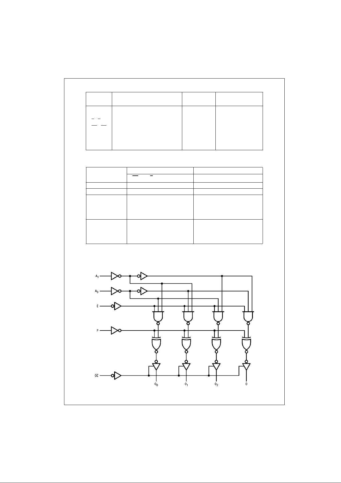
Unit Loading/Fan Out
Truth Table
(each half)
H = HIGH Voltage Level X = Immaterial
L = LOW Voltage Level Z = High Impedance
Logic Diagram (one half shown)
Please note that this diagram is provided o nly f or t he understanding of lo gic operations and should not be used to estimate propagation delays.
Pin Names Description
U.L.
Input I
IH/IIL
HIGH/LOW
Output I
OH/IOL
A0a–A
1a
Side A Address Inputs 1.0/1.0 20 µA/−0.6 mA
A
0b–A1b
Side B Address Inputs 1.0/1.0 20 µA/−0.6 mA
E
a
, E
b
Enable Inputs (Active LOW) 1.0/1.0 20 µA/−0.6 mA
OE
a
, OE
b
Output Enable Inputs (Active LOW) 1.0/1.0 20 µA/−0.6 mA
P
a
, P
b
Polarity Control Inputs 1.0/1.0 20 µA/−0.6 mA
O
0a–O3a
Side A 3-STATE Outputs 150/40 (33.3) −3 mA/24 mA (20 mA)
O
0b–O3b
Side B 3-STATE Outputs 150/40 (33.3) −3 mA/24 mA (20 mA)
Function
Inputs Outputs
OE
E
A
1
A
0
O
0
O
1
O
2
O
3
High Impedance H X X X Z Z Z Z
Disable L H X X O
n
= P
Active HIGH L L L L H L L L
Output L L L H L H L L
(P = L) LLHLLLHL
LLHH L L LH
Active LOW L L L L L H H H
Output L L L H H L H H
(P = H) L L H L H H L H
LLHHHHHL
 Loading...