

Fairchild Semiconductor 74F524PC, 74F524CW, 74F524SCX, 74F524SC Datasheet
© 1999 Fairchild Semiconductor Corporation DS009546 www.fairchildsemi.com
April 1988
Revised August 1999
74F524 8-Bit Registered Comparator
74F524
8-Bit Registered Comparator
General Description
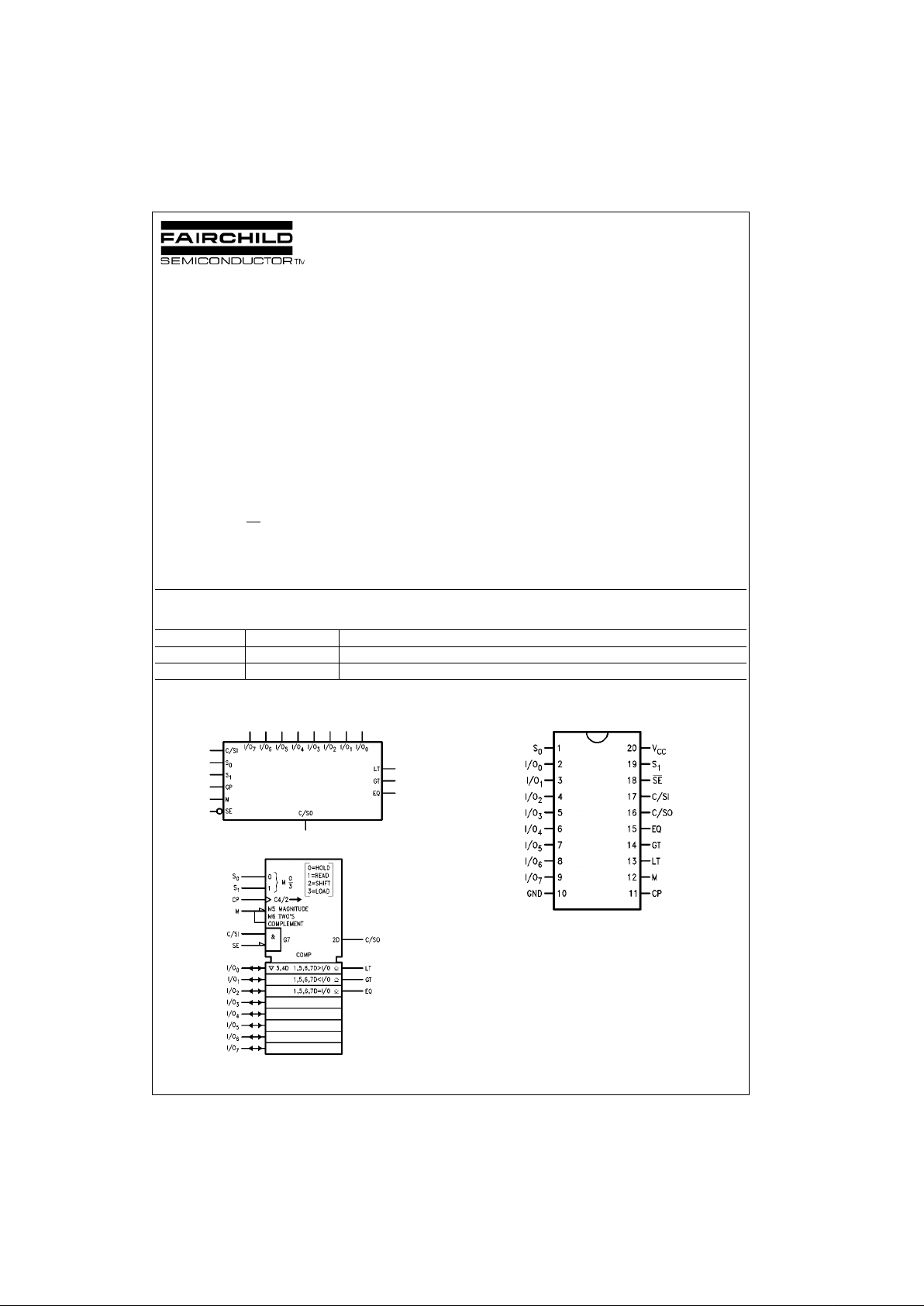
The 74F524 is an 8-bit bidirectional register with parallel
input and output p lus serial input and output progressing
from LSB to MSB. A ll data inputs, s erial and paralle l, are
loaded by the rising edge of the input clock. The device
functions are controlled by two control lines (S
0
, S1) to execute shift, load, hold and read out.
An 8-bit comparator exam ines the da ta store d in the reg is-
ters and on the data bus. Three true-HIGH, open-c ollector
outputs representing “register equal to bus”, “register
greater than bus” and “register less than bus” are provided.
These outputs can be disabled to the OFF state by the use
of Status Enable ( SE
). A mode control has also been pr ovided to allow twos complement as well as magnitude compare. Linking inputs are provided for expansion to long er
words.
Features
■ 8-Bit bidirectional register with bus-oriented input-output
■ Independent serial input-output to register
■ Register bus comparato r with “equal to”, “greater th an”
and “less than” outputs
■ Cascadable in groups of eight bits
■ Open-collector comparator outputs for AND-wired
expansion
■ Twos complement or magnitude compare
Ordering Code:
Devices also availab le in Tape and Reel. Specify by appending th e s uffix let t er “X” to the ordering code.
Logic Symbols
IEEE/IEC
Connection Diagram
Order Number Package Number Package Description
74F524SC M20B 20-Lead Small Outline Integrated Circuit (SOIC), JEDEC MS-013, 0.300 Wide
74F524PC N20A 20-Lead Plastic Dual-In-Line Package (PDIP), JEDEC MS-001, 0.300 Wide
www.fairchildsemi.com 2
74F524
Unit Loading/Fan Out
Note 1: OC = Open Collector
Number Representation Select Table
Select Truth Table
Status Truth Table
(Hold Mode)
1 = HIGH if data are equal, ot herwise LOW
H = HIGH Voltage Level
L = LOW Voltage Level
X = Immaterial
Pin Names Description
U.L.
Input I
IH/IIL
HIGH/LOW
Output I
OH/IOL
S0, S
1
Mode Select Inputs 1.0/1.0 20 µA/−0.6 mA
C/SI Status Priority or Serial Data Input 1.0/1.0 20 µA/−0.6 mA
CP Clock Pulse Input (Active Rising Edge) 1.0/1.0 20 µA/−0.6 mA
SE
Status Enable Input (Active LOW) 1.0/1.0 20 µA/−0.6 mA
M Compare Mode Select Input 1.0/1.0 20 µA/−0.6 mA
I/O
0
–I/O7Parallel Data Inputs or 3.5/1.083 70 µA/−0.65 mA
3-STATE Parallel Data Outputs 150/40 (33. 3) −3 mA/24 mA (20 mA)
C/SO Status Priority or Serial Data Output 50/33.3 −1 mA/20 mA
LT Register Less Than Bus Output OC (Note 1) /33.3 (Note 1) /20 mA
EQ Register Equal Bus Output OC(Note 1) /33.3 (Note 1) /20 mA
GT Register Greater Than Bus Output OC(Note 1) /33.3 (Note 1) /20 mA
MOperation
L Magnitude Compare
H Twos Complement Compare
S
0
S
1
Operation
L L Hold—Retains Data in Shift Register
L H Read—Read Contents in Register onto Data Bus,
Data Remains in Register Unaffected by Clock
H L Shift—Allows Serial Shifting on Next Rising Clock Edge
H H Load—Load Data on Bus into Register
Inputs Outputs
SE
C/SI Data Comparison EQ GT LT C/SO
HH X HHH1
LL O
A–OH
> I/O0–I/O
7
LHHL
XL O
A–OH
= I/O0–I/O
7
HHHL
HL O
A–OH
< I/O0–I/O
7
LHHL
HH O
A–OH
> I/O0–I/O
7
LHLL
HH O
A–OH
= I/O0–I/O
7
HLLH
LH O
A–OH
< I/O0–I/O
7
LLHL
3 www.fairchildsemi.com
74F524
Functional Description
The 74F524 contains eight D-type flip-flops connected as a
shift register with provision for ei ther pa rallel or seri al loading. Parallel data may be read from or loaded into the registers via the data bus I/O
0
–I/O7. Serial data is enter ed fro m
the C/SI input and may be shifted into the register and out
through the C/SO output. Both parallel and serial data entry
occur on the rising edge of the input clock (CP). The operation of the shift reg ister i s cont rolle d by t wo s ignals S
0
and
S
1
according to the Select Truth Table. The 3-STATE parallel output buffers are enabled only in the Read mode.
One port of an 8-bit compara tor is attached to the data bus
while the other port is tied to the outputs of the internal register. Three active-OFF, open-collector outputs indicate
whether the contents held in th e shift register are “great er
than”, (GT), “less than” (LT), or “equal to” (E Q) the dat a on
the input bus. A HI GH signal on the Status Ena ble (SE
)
input disables these outputs to the OFF state. A mode control input (M) allows selection between a straightforward
magnitude compare or a comparison between twos complement numbers.
For “greater than” or “les s than” detection, the C/SI input
must be held HIGH, as indicat ed in the Status Truth Table.
The internal logic is arra nged such that a LOW signal on
the C/SI input disables the “great er than” and “less than”
outputs. The C/SO output will be forced HIGH if the “equal
to” status condition exists, otherwise C/SO will be held
LOW. These facilities enable the 74F524 to be cascaded
for word length greater than eight bits.
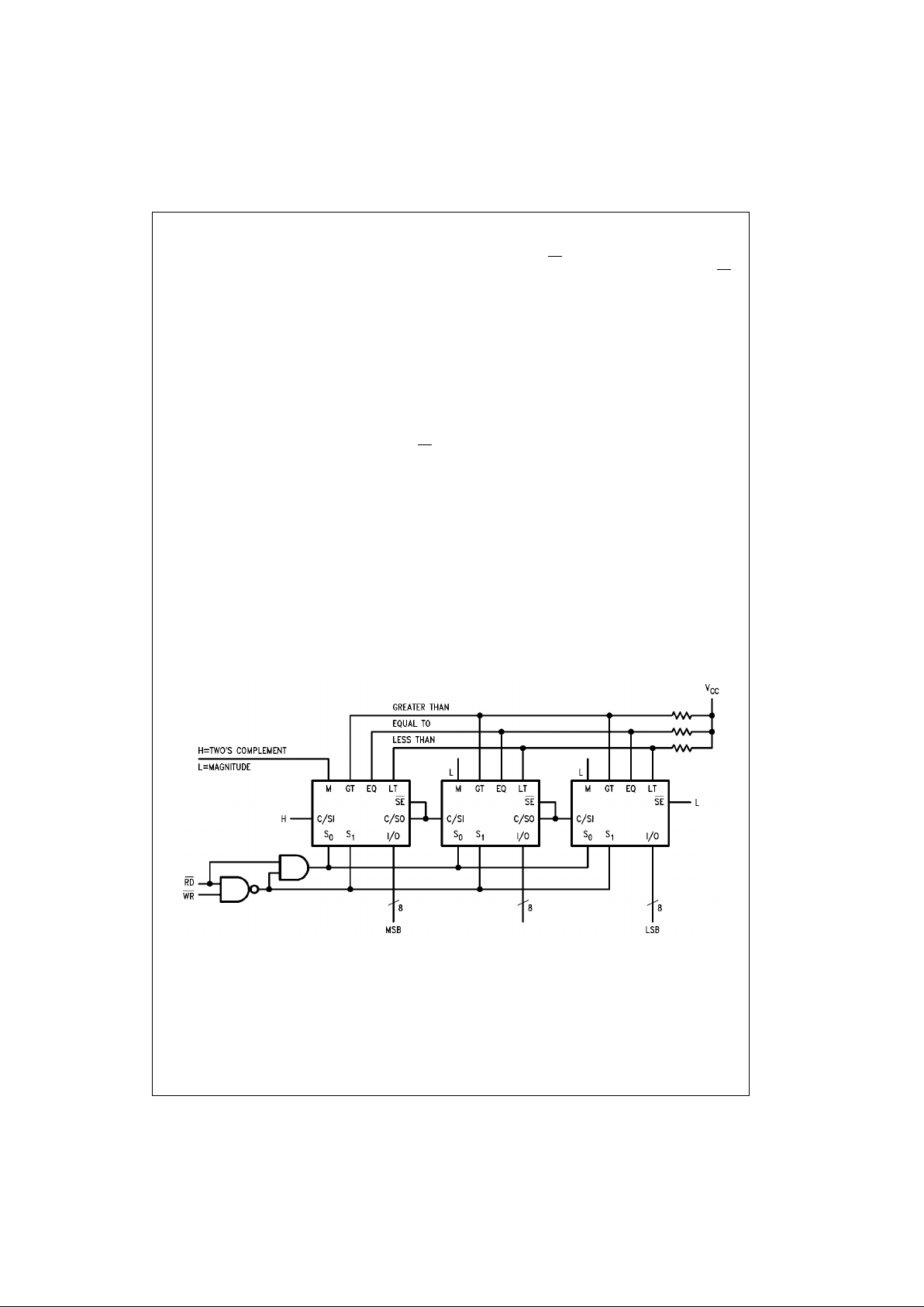
Word length expansion (in groups of eight bits) can be
achieved by connecting the C/SO output of the more signif-
icant byte to the C/SI input of the next less significant byte
and also to its own SE
input (see Figure 1). Th e C /SI i n pu t
of the most significant device is held HI GH while the SE
input of the least significant device is held LOW. The corresponding status outputs are AND-wired together. In the
case of twos complement nu mbe r co mpa re , only th e M ode
input to the most signifi cant device should be HIGH. T he
Mode inputs to all other cascaded devices are held LOW.
Suppose that an inequality condition is detected in the
most significant device. Assu ming that the byte stored in
the register is greater than the byte on the data bus, the EQ
and LT outputs will be pulled LOW and the GT output will
float HIGH. Also the C/SO outp ut of the most significant
device will be forced LOW, disabling the subsequent
devices but enabling its own status outputs. The correct
status condition is thus indicated. The same applies if the
registered byte is less th an th e data byte, only in this case
the EQ and GT outputs go LOW and LT output floats HIGH.
If an equality condi tion is detected in the most significant
device, its C/SO outpu t is forced HIGH. This ena bles the
next less significant device and also disables its own status
outputs. In this way, the status ou tput priority is handed
down to the next less significant device which now effectively becomes the most si gnificant byte. The worst case
propagation delay for a compare operation involving “n”
cascaded 74F524s will be when an equality condition is
detected in all but the least significant byte. In this case, the
status priority has to ripple all the way down the chain
before the correct status outp ut is established. Typically,
this will take 35 + 6(n−2) ns.
Function Diagram
FIGURE 1. Cascading 74F524s for Comparing Longer Words
 Loading...