

© 1999 Fairchild Semiconductor Corporation DS009545 www.fairchildsemi.com
April 1988
Revised August 1999
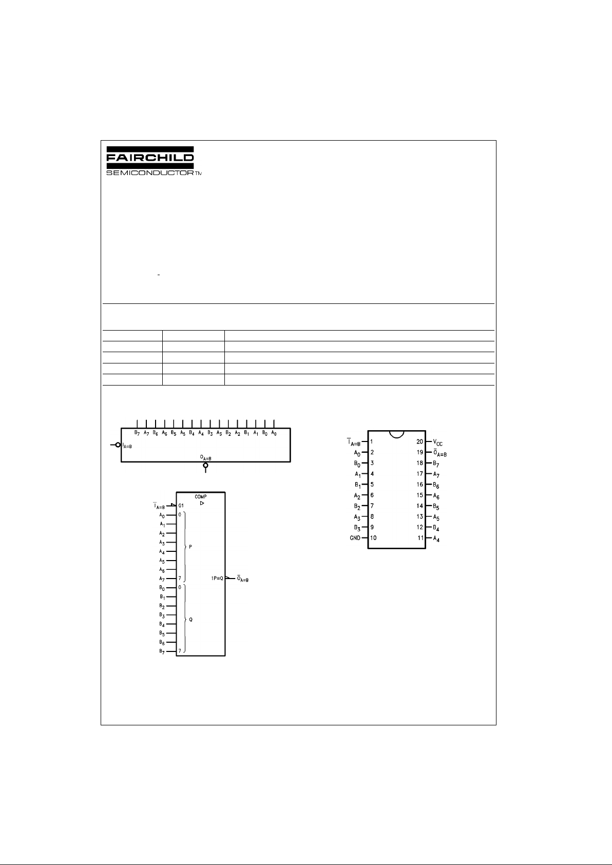
74F521 8-Bit Identity Comparator
74F521
8-Bit Identity Comparator
General Description
The 74F521 is a n expandable 8-bit comparator. It compares two words of up to eight bits eac h and provides a
LOW output when the two words match bit for bit. The
expansion input I
A=B
also serves as an active LOW enable
input.
Features
■ Compares two 8-bit words in 6.5 ns typ
■ Expandable to any word length
■ 20-pin package
Ordering Code:
Devices also availab le in Tape and Reel. Specify by appending th e s uffix let t er “X” to the ordering code.
Logic Symbols
IEEE/IEC
Connection Diagram
Order Number Package Number Package Description
74F521SC M20B 20-Lead Small Outline Integrated Circuit (SOIC), JEDEC MS-013, 0.300 Wide
74F521SJ M20D 20-Lead Small Outline Package (SOP), EIAJ TYPE II, 5.3mm Wide
74F521MSA MSA20 20-Lead Shrink Small Outline Package (SSOP), EIAJ TYPE II, 5.3mm Wide
74F521PC N20A 20-Lead Plastic Dual-In-Line Package (PDIP), JEDEC MS-001, 0.300 Wide
www.fairchildsemi.com 2
74F521
Unit Loading/Fan Out
Truth Table
H = HIGH Voltage Level
L = LOW Voltage Level
Note 1: A
0
= B0, A1 = B1, A2 = B2, etc.
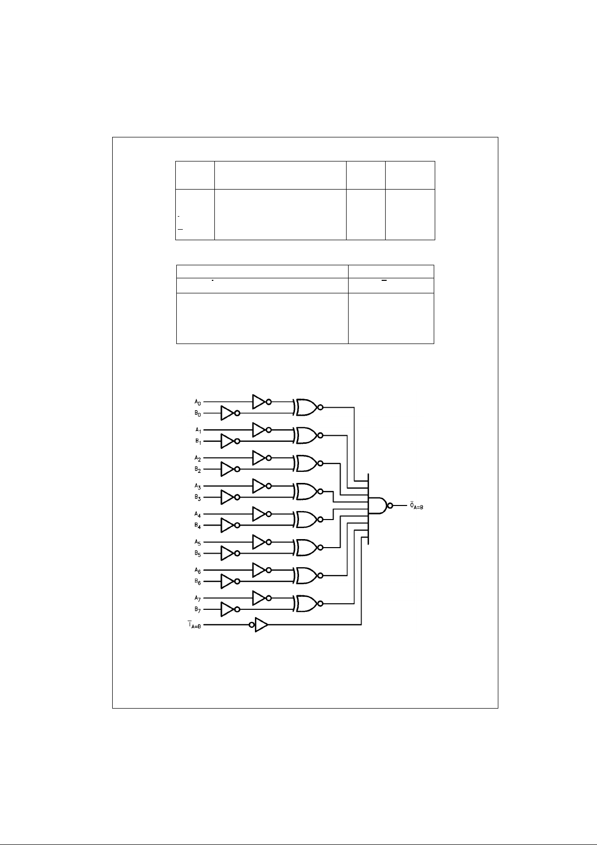
Logic Diagram
Please note that this diagram is provided o nly f or t he understanding of lo gic operations and should not be used to estimate propagation delays.
Pin Names Description
U.L. Input I
IH/IIL
HIGH/LOW Output IOH/I
OL
A0–A
7
Word A Inputs 1.0/1.0 20 µA/−0.6 mA
B
0–B7
Word B Inputs 1.0/1.0 20 µA/−0.6 mA
I
A=B
Expansion or Enable Input (Active LOW) 1.0/1.0 20 µA/−0.6 mA
O
A=B
Identity Output (Active LOW) 50/33.3 −1 mA/20 mA
Inputs Output
I
A = B
A, B O
A = B
LA = B (Note 1) L
LA ≠ BH
HA = B (Note 1) H
HA ≠ BH
3 www.fairchildsemi.com
74F521
Absolute Maximum Ratings(Note 2) Recommended Operating
Conditions
Note 2: Absolute maximum ratings are values beyon d which the device
may be damaged or have its useful life impaired . Functional operation
under these condit ions is not implied.
Note 3: Either voltage limit or curren t limit is sufficient to protect in puts.
DC Electrical Characteristics
Storage Temperature −65°C to +150°C
Ambient Temperature under Bias −55°C to +125°C
Junction Temperature under Bias −55°C to +150°C
V
CC
Pin Potential to Ground Pin −0.5V to +7.0V
Input Voltage (Note 3) −0.5V to +7.0V
Input Current (Note 3) −30 mA to +5.0 mA
Voltage Applied to Output
in HIGH State (with V
CC
= 0V)
Standard Output −0.5V to V
CC
3-STATE Output −0.5V to +5.5V
Current Applied to Output
in LOW State (Max) twice the r ated I
OL
(mA)
Free Air Ambi ent Temperature 0°C to +70°C
Supply Voltage +4.5V to +5.5V
Symbol Parameter Min Typ Max Units
V
CC
Conditions
V
IH
Input HIGH Voltage 2.0 V Recognized as a HIGH Signal
V
IL
Input LOW Voltage 0.8 V Recognized as a LOW Signal
V
CD
Input Clamp Diode Voltage −1.2 V Min IIN = −18 mA
V
OH
Output HIGH 10% V
CC
2.5 V Min IOH = −1 mA
Voltage 5% V
CC
2.7 IOH = −1 mA
V
OL
Output LOW 10% V
CC
0.5 V Min IOL = 20 mA
Voltage
I
IH
Input HIGH Current 5.0 µAMaxVIN = 2.7V
I
BVI
Input HIGH Current
7.0 µAMaxVIN = 7.0V
Breakdown Test
I
CEX
Output HIGH
50 µAMaxV
OUT
= V
CC
Leakage Current
V
ID
Input Leakage
4.75 V 0.0
IID = 1.9 µA
Test All Other Pins Grounded
I
OD
Output Leakage
3.75 µA0.0
V
IOD
= 150 mV
Circuit Current All Other Pins Grounded
I
IL
Input LOW Current −0.6 mA Max VIN = 0.5V
I
OS
Output Short-Circuit Current −60 −150 mA Max V
OUT
= 0V
I
CCH
Power Supply Current 21 32 mA Max VO = HIGH
 Loading...