Fairchild Semiconductor 74F402PC Datasheet

74F402
Serial Data Polynomial Generator/Checker
74F402 Serial Data Polynomial Generator/Checker
April 1988
Revised August 1999
General Description
The 74F402 expandable Serial Data Polynomial generator/
checker is an expandable versio n of the 74F401. It provides an advanced tool for th e implem entation of th e most
widely used error detection scheme in serial dig ital handling systems. A 4-bit control input sel ects one-of-six generator polynomials. The list of polynomials includes CRC16, CRC-CCITT and Ethernet, as well as three other
standard polynomials (56
Individual clear and pre set inputs are provided for floppy
disk and other applications. The Error output indicates
whether or not a transmission error has occurred. The
CWG Control input inhibits feedback during check word
transmission. The 74F402 is compatible with FAST
devices and with all TTL families.
th
order, 48th order, 32nd order).
Features
■ Guaranteed 30 MHz data rate
■ Six selectable polynomials
■ Other polynomials available
■ Separate preset and clear controls
■ Expandable
■ Automatic right justification
■ Error output open collector
■ Typical applications: Floppy and othe r disk stora ge sys-
tems Digital cassette and cartridge systems Data communication systems
Ordering Code:
Order Number Package Number Package Description
74F402PC N16E 16-Lead Plastic Dual-In-Line Package (PDIP), JEDEC MS-001, 0.300 Wide
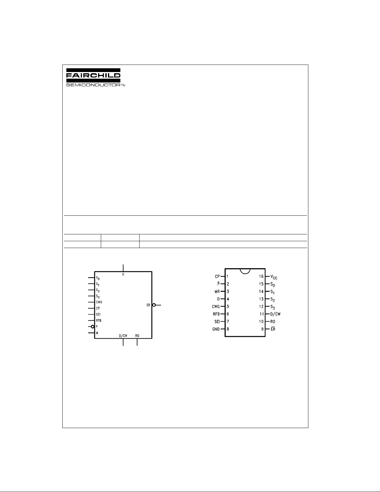
Logic Symbol Connection Diagram
FAST is a regist ered trademark of Fair c hild Semiconductor Corporation.
Ethernet is a registe red trademark of Xerox C orporation.
© 1999 Fairchild Semiconductor Corporation DS009535 www.fairchildsemi.com

Unit Loading/Fan Out
74F402
Note 1: Open Collector
Pin Names Description
S0–S
CWG Check Word Generate Input 1.0/0.67 20 µA/−0.4 mA
D/CW Serial Data/Check Word 285(100)/13.3(6.7) −5.7 mA(−2 mA)/8 mA (4 mA)
D Data Input 1.0/0.67 20 µA/−0.4 mA
ER
RO Register Output 285(100)/13.3(6.7) −5.7 mA(−2 mA)/8 mA (4 mA)
CP Clock Pulse 1.0/0.67 20 µA/−0.4 mA
SEI Serial Expansion Input 1.0/0.67 20 µA/−0.4 mA
RFB Register Feedback 1.0/0.67 20 µA/−0.4 mA
MR Master Reset 1.0/0.67 20 µA/−0.4 mA
P
Polynomial Select Inputs 1.0/0.67 20 µA/−0.4 mA
3
Error Output (Note 1) /26.7(13.3) (Note 1) /16 mA (8 mA)
Preset 1.0/0.67 20 µA/−0.4 mA
Functional Description
The 74F402 Serial Data Polynomial Generato r/Checker is
an expandable 16-bit programmable device which operates on serial data streams and provides a means of
detecting transmission er rors. Cyclic encod ing and decoding schemes for err or detection are based on poly nomial
manipulation in m odulo arithmetic . For encoding , the data
stream (message polynomial) is divided by a selected polynomial. This division results in a remainder (or residue)
which is appended t o th e m essa ge a s che ck bi t s. Fo r e rro r
checking, the bit st ream containing both data and check
bits is d ivided by the same selected polynomial. If there are
no detectable errors, th is division results in a zero remain der. Although it is possible to choose many generating
polynomials of a given de gre e, stan dar ds exist tha t spe cify
a small number of usefu l polynomials. The 7 4F402 implements the polynomials listed in Table 1 by applying the
appropriate logic levels to the select pins S
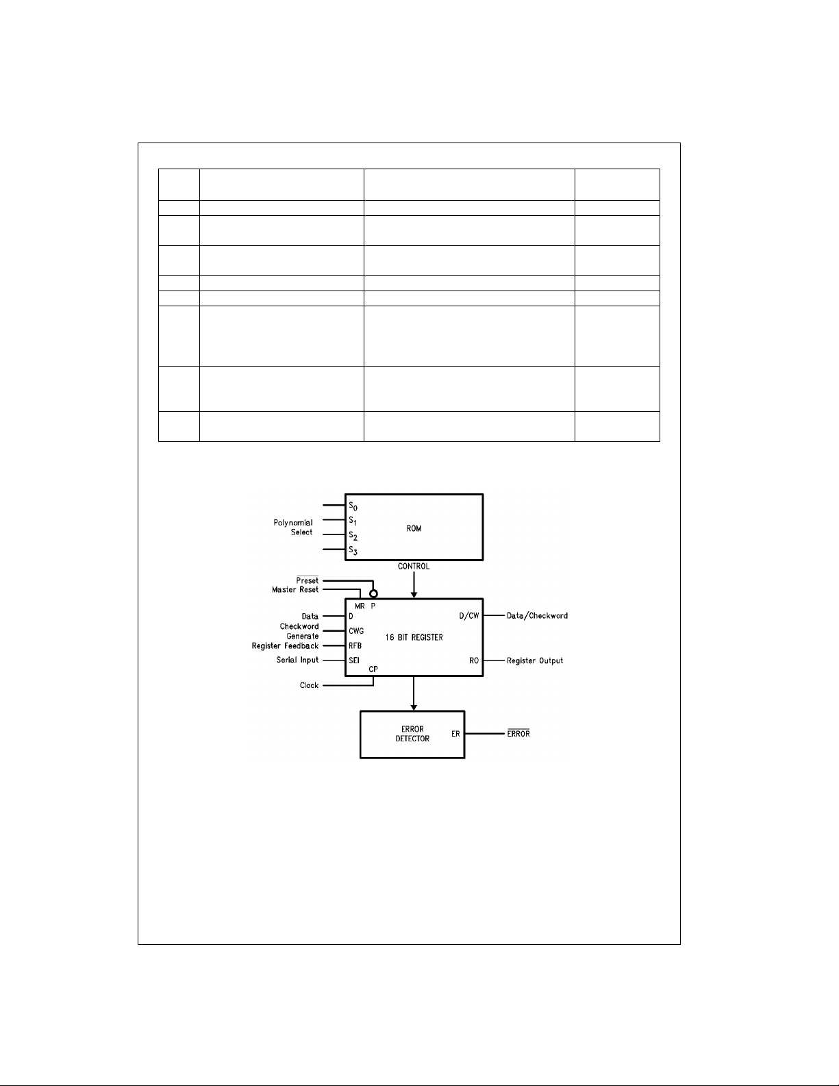
The 74F402 consists of a 16-bit register, a Read Only
Memory (ROM) and associated control circuitry as show n
in the Block Diagram. The polynomial control code presented at inputs S
selecting the desir ed polynom ial o r part of a p olyno mia l by
establishing shift mode operation on the register with
Exclusive OR (XOR) gates at appropriate inputs. To generate the check bits, the data stre am is entered via the Data
Inputs (D), using the LOW-to-HIGH transit ion of the Clock
Input (CP). This data is gated with the most significant
Register Output (RO) via the Register Feedback Input
(RFB), and controls the XOR gates. The Check Word Gen-
, S1, S2 and S3 is decoded by the ROM,
0
, S1, S2 and S3.
0
U.L.
HIGH/LOW
erate (CWG) mu st be held HIGH while t he data is being
entered. After the last data bit is entered, the CWG is
brought LOW and the check b its are shift ed ou t of the register(s) and appended to the data bits (no external gating is
needed).
To check an incoming messa ge for errors, both the data
and check bits are enter ed through the D Input with the
CWG Input held HIGH. The Error Output becom es valid
after the last check bit has been entered into the ’F402 by a
LOW-to-HIGH transition of CP, with the exception of the
Ethernet polynomial (see Applications paragraph). If no
detectable errors ha ve occurred during the data transmission, the resultant internal register bits are all LOW and the
Error Output (ER
occurred, ER
to-HIGH transition o f CP or until th e device has b een preset or reset.
A HIGH on the Master Reset Input (MR) asynchronous ly
clears the entire register. A LOW on the Preset Input (P
asynchronously sets the enti re register with the exception
of:
1. The Ethernet residue se lection, in which the regist ers
containing the non-zero res idue are cleared;
2. The 56th order polynomial, in which the 8 least significant register bits of the least significant device are
cleared; and,
3. Register S = 0, in which all bits are cleared.
) is HIGH. If a detectable error has
is LOW. ER remains valid until the next LOW-
Input I
Output I
IH/IIL
OH/IOL
)
www.fairchildsemi.com 2

TABLE 1.
Hex
S
3
Select Code
S
S
2
S
1
0
Polynomial Remarks
0LLLL0 S = 0
CHHLLX
DHHLHX
EHHHLX
FHHHHX
7LHHHX
BHLHHX
3LLHHX
2LLHLX
4LHLLX
8HLLLX
5LHLHX
32+X26+X23+X22+X16
12+X11+X10+X8+X7+X5+X4+X2
32+X31+X27+X26+X25+X19+X16
15+X13+X12+X11+X9+X7+X6+X5+X4+X2
16+X15+X2
16+X12+X5
56+X55+X49+X45+X41
39+X38+X37+X36+X31
22+X19+X17+X16+X15+X14+X12+X11+X9
5
+X+1
48+X36+X35+
+1 CRC-16
+1 CRC-CCITT
+ Ethernet
+X+1 Polynomial
+ Ethernet
+
+ 56th
9HLLHX23+X21+ 48th
1LLLHX
6LHHLX
AHLHLX
15+X13+X8+X2
32+X23+X21
11+X2
+1Order
+ 32nd
+1Order
Block Diagram
74F402
+X+1 Residue
+ Order
3 www.fairchildsemi.com
 Loading...