© 1999 Fairchild Semiconductor Corporation DS009533 www.fairchildsemi.com
April 1988
Revised August 1999
74F398 • 74F399 Quad 2-Port Register
74F398 • 74F399
Quad 2-Port Register
General Description
The 74F398 and 7 4F399 are the logical equi valents of a
quad 2-input multiplexe r feeding into four edge-triggered
flip-flops. A common Select input determines which of the
two 4-bit words is accep ted. The selected da ta enters the
flip-flops on the risin g ed ge of th e cl ock . Th e 74 F3 99 i s t he
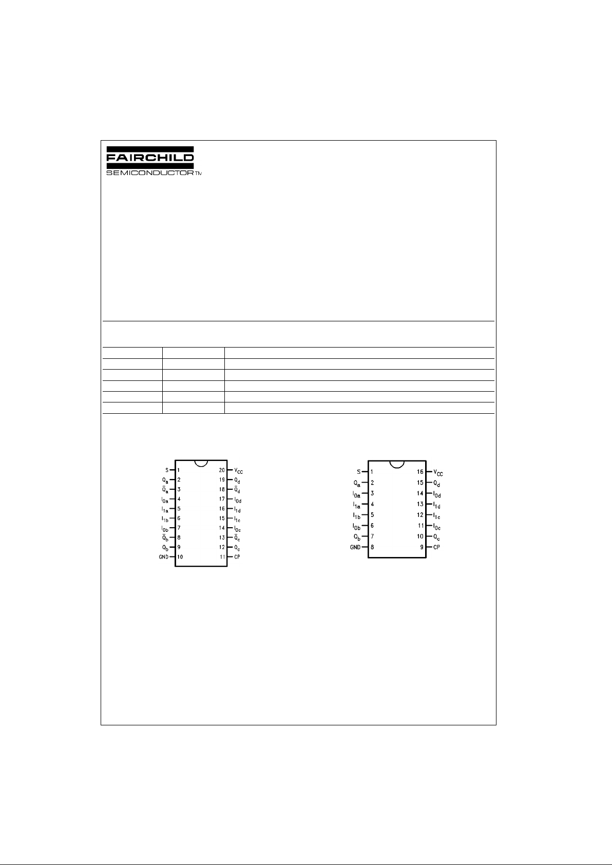
16-pin version of the 74F398, with only the Q outputs of the
flip-flops available.
Features
■ Select inputs from two data sources
■ Fully positive edge-triggered operation
■ Both true and complement outputs—74F398
Ordering Code:
Device also available in Tape and Reel. Specify by appending s uffix let te r “X” to the ordering code.
Connection Diagrams
74F398 74F399
Order Number Package Number Package Description
74F398SC M20B 20-Lead Small Outline Integrated Circuit (SOIC), JEDEC MS-013, 0.300” Wide Body
74F398PC N20A 20-Lead Plastic Dual-In-Line Package (PDIP), JEDEC MS-001, 0.300” Wide
74F399SC M16A 16-Lead Small Outline Integrated Circuit (SOIC), JEDEC MS-012, 0.150” Narrow Body
74F399SJ M16D 16-Lead Small Outline Package (SOP), EIAJ TYPE II, 5.3mm Wide
74F399PC N16E 16-Lead Plastic Dual-In-Line Package (PDIP), JEDEC MS-001, 0.300” Wide

www.fairchildsemi.com 2
74F398 • 74F399
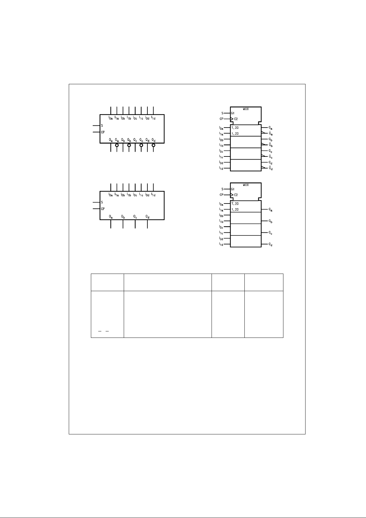
Logic Symbols
74F398
74F399
IEEE/IEC
74F398
74F399
Unit Loading/Fan Out
Pin Names Description
U.L.
Input I
IH/IIL
HIGH/LOW
Output I
OH/IOL
S Common Select Input 1.0/1.0 20 µA/−0.6 mA
CP Clock Pulse Input (Active Rising Edge) 1.0/1.0 20 µA/−0.6 mA
I
0a–I0d
Data Inputs from Source 0 1.0/1.0 20 µA/−0.6 mA
I
1a–I1d
Data Inputs from Source 1 1.0/1.0 20 µA/−0.6 mA
Q
a–Qd
Register True Outputs 50/33.3 −1 mA/20 mA
Q
a–Qd
Register Complementary Outputs (74F398) 50/33.3 −1 mA/20 mA

3 www.fairchildsemi.com
74F398 • 74F399
Functional Description
The 74F398 and 74F399 are high-speed quad 2-port registers. They select four bits of data from either of two sources
(Ports) under control of a com mon Select input (S). The
selected data is transferred to a 4-b it output register synchronous with the LOW-to-HIGH transition of the Clock
input (CP). The 4-bit D-typ e output register is fully edgetriggered. The Data inputs (I
0x
, I1x) and Select input (S )
must be stable only a setup time prior to and hold time after
the LOW-to-HIGH transition of the Clock input for predictable operation. The 74F398 has both Q and Q
outputs.
Function Table
H = HIGH Voltage Level
L = LOW Voltage Level
h = HIGH Voltage Level one setup time prior to the LOW-to-HIGH
clock transition
I = LOW Voltage Level one setup tim e prior to the LOW-to-HIGH
clock transition
X = Immaterial
Note 1: 74F398 only
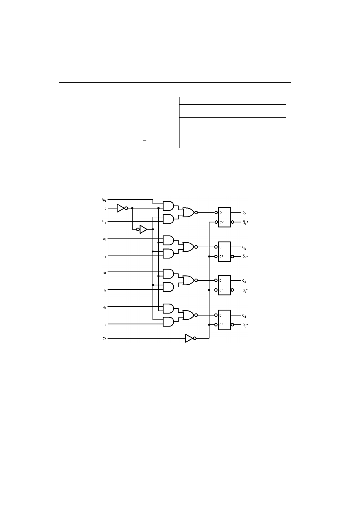
Logic Diagram
*F398 Only
Please note that this d iagram is provided only f or t he understanding of lo gic operations and should not be used to estimat e propagation delays.
Inputs Outputs
SI
0
I
1
QQ
(Note 1)
IIXLH
IhXHL
hX I LH
hX hHL
 Loading...