

Fairchild Semiconductor 74F382SJ, 74F382SCX, 74F382SC, 74F382PC Datasheet
© 1999 Fairchild Semiconductor Corporation DS009529 www.fairchildsemi.com
May 1988
Revised August 1999
74F382 4-Bit Arithmetic Logic Unit
74F382
4-Bit Arithmetic Logic Unit
General Description
The 74F382 p er f or ms t h re e ar it h me ti c an d th r ee lo gic operations on two 4-bit w ords, A and B. Two additional S elect
input codes force the F unction outputs LOW or HIGH. An
Overflow output is p rovided for conven ience in twos com plement arithmetic. A Carry output is provided for ripple
expansion. For high-speed expansion using a Carry Lookahead Generator, refer to the 74F381 data sheet.
Features
■ Performs six arithmetic and logic functions
■ Selectable LOW (clear) and HIGH (preset) functions
■ LOW input loading minimizes drive requirements
■ Carry output for ripple expansion
■ Overflow output for twos complement arithmetic
Ordering Code:
Devices also availab le in Tape and Reel. Specify by appending th e s uffix let t er “X” to the ordering code.
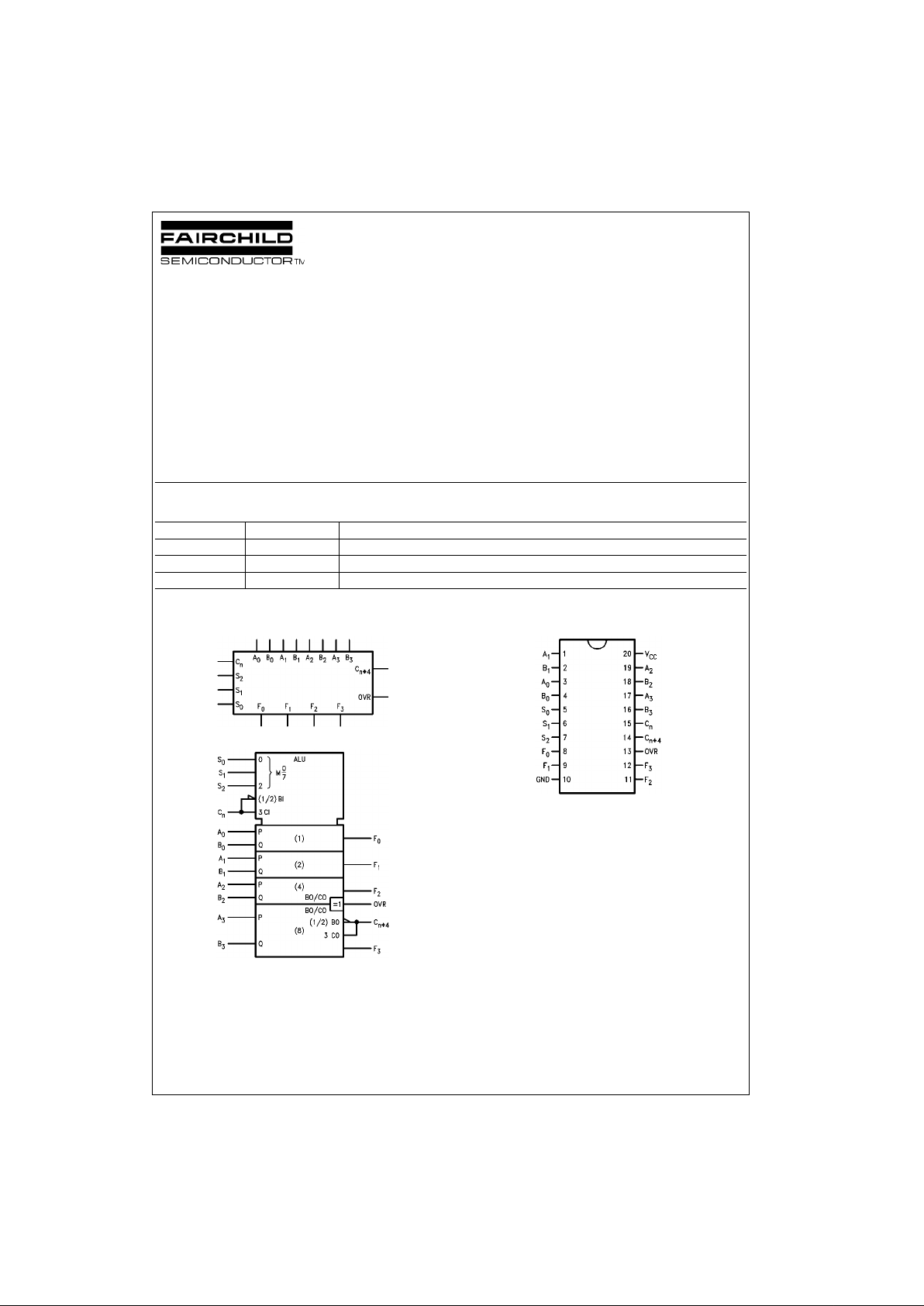
Logic Symbols
IEEE/IEC
Connection Diagram
Order Number Package Number Package Description
74F382SC M20B 20-Lead Small Outline Integrated Circuit (SOIC), JEDEC MS-013, 0.300 Wide
74F382SJ M20D 20-Lead Small Outline Package (SOP), EIAJ TYPE II, 5.3mm Wide
74F382PC N20A 20-Lead Plastic Dual-In-Line Package (PDIP), JEDEC MS-001, 0.300 Wide
www.fairchildsemi.com 2
74F382
Unit Loading/Fan Out
Functional Description
Signals applied to the Select inputs S0–S2 determine the
mode of operation, as indicated in the Function Select
Table. An extensive listing of input and output levels is
shown in the Truth Table. The circuit perform s the arithmetic functions for eit her active HIGH or active LOW o perands, with output levels in the same convention. In the
Subtract operating m odes, it is necessa ry to force a carry
(HIGH for active HIGH operands, LOW for active LOW
operands) into the C
n
input of the least significant package.
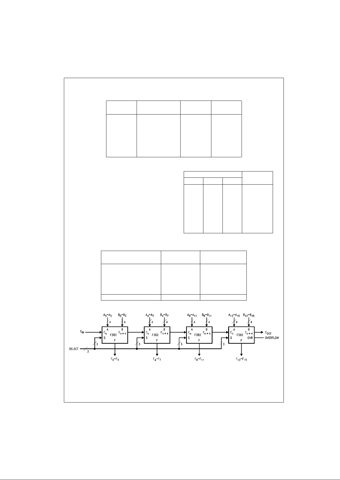
Ripple expansion is illustrated in Figure 2. The overflow
output OVR is the Exclusive-OR of C
n + 3
and C
n + 4
; a
HIGH signal on OVR indica tes overflow in twos complement operation. Typical delays fo r Figure 2 are given in
Figure 1.
Function Select Table
H = HIGH Voltage Level
L = LOW Voltage Level
FIGURE 1. 16-Bit Delay Tabulation
FIGURE 2. 16-Bit Ripply Carry ALU Expansion
Pin Names Description
U.L.
Input I
IH/IIL
HIGH/LOW
Output I
OH/IOL
A0–A
3
A Operand Inputs 1.0/4.0 20 µA/−2.4 mA
B
0–B3
B Operand Inputs 1.0/4.0 20 µA/−2.4 mA
S
0–S2
Function Select Inputs 1.0/1.0 20 µA/−0.6 mA
C
n
Carry Input 1.0/5.0 20 µA/−3.0 mA
C
n + 4
Carry Output 50/33.3 −1 mA/20 mA
OVR Overflow Output 50/33.3 −1 mA/20 mA
F
0–F3
Function Outputs 50/33.3 −1 mA/20 mA
Select
Operation
S
0
S
1
S
2
L L L Clear
H L L B Minus A
L H L A Minus B
HHLA Plus B
LLHA ⊕ B
HLHA + B
LHHAB
HHHPreset
Path Segment
Toward Output
F
C
n + 4
, OVR
A
1
or B1 to C
n + 4
6.5 ns 6.5 ns
C
n
to C
n + 4
6.3 ns 6.3 ns
C
n
to C
n + 4
6.3 ns 6.3 ns
C
n
to F 8.1 ns —
C
n
to C
n + 4
, OVR — 8.0 ns
Total Delay 27.2 ns 27.1 ns
3 www.fairchildsemi.com
74F382
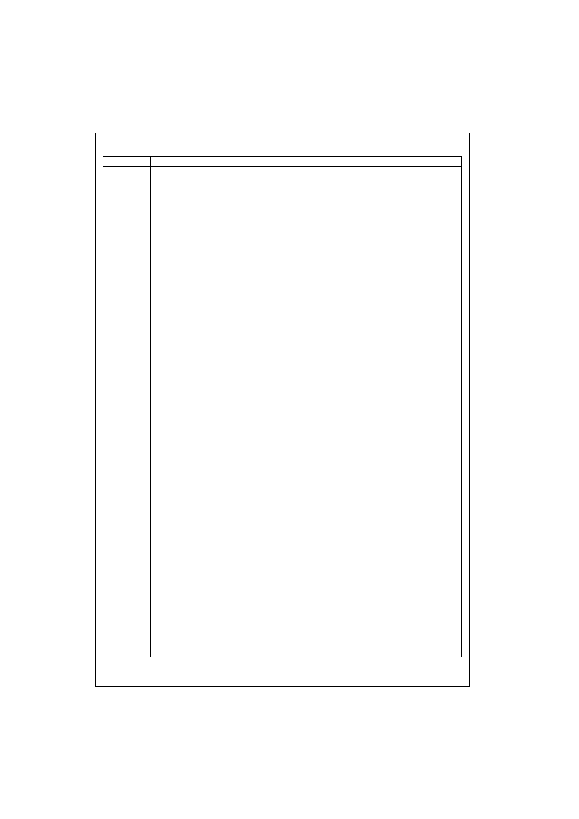
Truth Table
H = HIGH Voltage Level L = LOW Voltage Level X = Immaterial
Inputs Outputs
Function
S
0
S
1
S
2
C
n
A
n
B
n
F
0
F
1
F
2
F
3
OVR
C
n + 4
CLEAR LLLLXXLLLLH H
HXXLLLLH H
B MINUS AHLLLLLHHHHL L
LLHLHHHL H
LHLLLLL L L
LHHHHHH L L
HLLLLLLL H
HLHHHHH L H
HHLHLL L L L
HHHL LL L L H
A MINUS B L H L L L L H H H H L L
LLHLLLL L L
LHLLHHH L H
LHHHHHH L L
HLLLLLLL H
HLHHLLL L L
HHLHHHH L H
HHHL LL L L H
A PLUS B HHLLLLLLLLL L
LLHHHHH L L
LHLHHHH L L
LHHLH H HL H
HLLHLLL L L
HLHLLLLL H
HHLLLLLL H
HHHHHHH L H
A ⊕ B LLHXLLLLLLL L
XLHHHHH L L
LHLHHHH L L
XHHLLLLH H
HHLHHHH H H
A + B HLHXLLLLLL L L
XLHHHHH L L
XHLHHHH L L
LHHHHHH L L
HHHHHHHH H
AB LHHXLLLLLLH H
XLHLLLLL L
XHLLLLLH H
LHHHHHH L L
HHHHHHHH H
PRESET H H H X L L H H H H L L
XLHHHHH L L
XHLHHHH L L
LHHHHHH L L
HHHHHHHH H
 Loading...