

Fairchild Semiconductor 74F365SCX, 74F365SC Datasheet
74F365
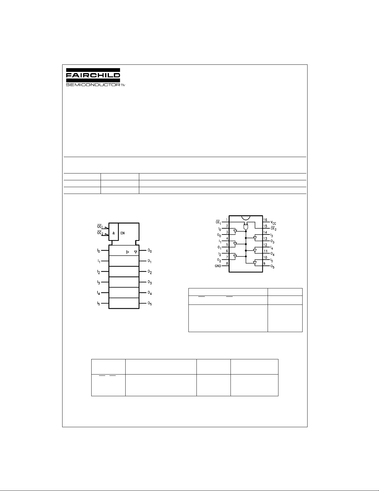
Hex Buffer/Driver with 3-STATE Outputs
74F365 Hex Buffer/Driver with 3-STATE Outputs
April 1988
Revised August 1999
General Description
The 74F365 is a hex buffer a nd line dri ver designed to be
employed as a memo ry and address driver, clock driver
and bus-oriented transmitter/receiver.
Features
■ 3-STATE buffer outputs
■ Outputs sink 64 mA
■ Bus-oriented
Ordering Code:
Order Number Package Number Package Description
74F365SC M16A 16-Lead Small Outline Integrated Circuit (SOIC), JEDEC MS-012, 0.150 Narrow
74F365PC N16E 16-Lead Plastic Dual-In-Line Package (PDIP), JEDEC MS-001, 0.300 Wide
Devices also availab le in Tape and Reel. Specify by appending th e s uffix let t er “X” to the ordering cod e.
Logic Symbol
IEEE/IEC
Connection Diagram
Function Table
Inputs Output
OE
1
LLL L
LLHH
XHX Z
HXX Z
L = LOW Voltage Level X = Immaterial
H = HIGH Voltage Level Z = High Impedance
OE
2
IO
Unit Loading/Fan Out
Pin Names Description
OE1, OE
I
n
O
n
© 1999 Fairchild Semiconductor Corporation DS009522 www.fairchildsemi.com
Output Enable Input (Active LOW) 1.0/0.033 20 µA/20 µA
2
Inputs 1.0/0.033 20 µA/20 µA
Outputs 600/106.6 (80) −12 mA/64 mA (48 mA)
U.L.
HIGH/LOW
Input I
Output I
IH/IIL
OH/IOL
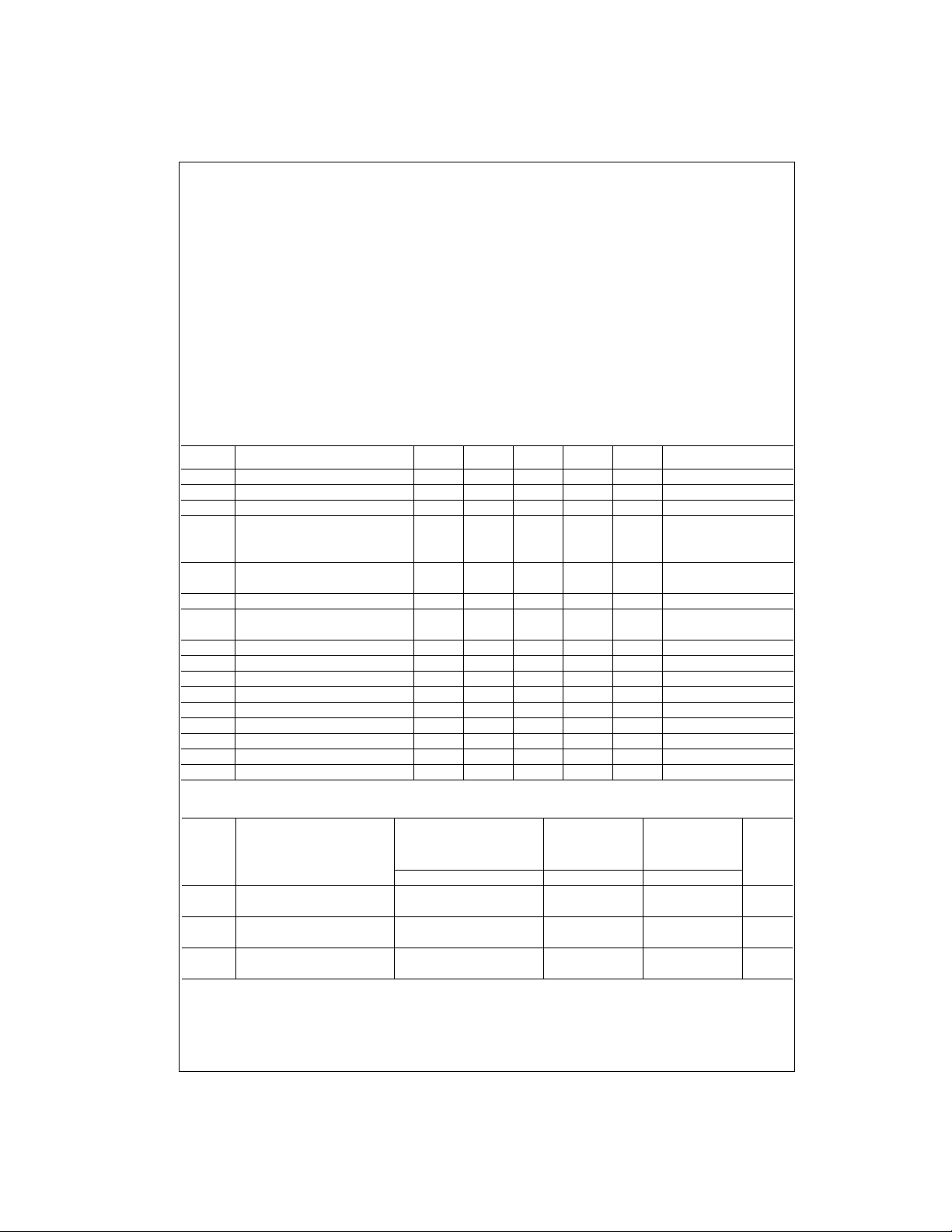
Absolute Maximum Ratings(Note 1) Recommended Operating
Storage Temperature −65°C to +150°C
74F365
Ambient Temperature under Bias −55°C to +125°C
Junction Temperature under Bias −55°C to +150°C
Pin Potential to Ground Pin −0.5V to +7.0V
V
CC
Input Voltage (Note 2) −0.5V to +7.0V
Input Current (Note 2) −30 mA to +5.0 mA
Voltage Applied to Output
in HIGH State (with V
CC
= 0V)
Standard Output −0.5V to V
3-STATE Output −0.5V to +5.5V
Current Applied to Output
in LOW State (Max) twice the rated I
OL
Conditions
Free Air Ambient Temperature 0°C to +70°C
Supply Voltage +4.5V to +5.5V
Note 1: Absolute maximum ratings are values beyond which the device
may be damaged or have its useful life impaired. Functional operation
CC
under these conditi ons is not implied.
Note 2: Either voltage limit or curren t limit is sufficient to protect in put s .
(mA)
DC Electrical Characteristics
Symbol Parameter Min Typ Max Units
V
IH
V
IL
V
CD
V
OH
V
OL
Input HIGH Voltage 2.0 V Recognized as a HIGH Signal
Input LOW Voltage 0.8 V Recognized as a LOW Signal
Input Clamp Diode Voltage −1.2 V Min IIN = −18 mA
Output HIGH 10% V
Voltage 10% V
5% V
Output LOW 10% V
2.4
CC
2.0 IOH = −15 mA
CC
2.7 IOH = −3 mA
CC
CC
0.55 V Min IOL = 64 mA
Voltage
I
I
I
I
I
I
I
I
I
I
I
IH
BVI
IL
OZH
OZL
OS
CEX
ZZ
CCH
CCL
CCZ
Input HIGH Current 20 µAMaxVIN = 2.7V
Input HIGH Current
Breakdown Test
100 µA0.0VIN = 7.0V
Input LOW Current −20 µAMaxVIN = 0.5V
Output Leakage Current 50 µAMaxV
Output Leakage Current −50 µAMaxV
Output Short-Circuit Current −100 −225 mA Max V
Output HIGH Leakage Current 250 µAMaxV
Bus Drainage Test 500 µA0.0VV
Power Supply Current 25 35 mA Max VO = HIGH
Power Supply Current 44 62 mA Max VO = LOW
Power Supply Current 35 48 mA Max VO = HIGH Z
AC Electrical Characteristics
Symbol Parameter
t
t
t
t
t
t
PLH
PHL
PZH
PZL
PHZ
PLZ
Propagation Delay 2.5 4.6 6.5 2.0 7.0 2.0 7.0
In to O
n
Enable Time 2.5 5.1 9.5 2.0 8.5 2.5 10.0
Disable Time 2.0 3.6 6.5 1.5 6.5 2.0 7.0
TA = +25°CT
VCC = +5.0V VCC = +5.0V VCC = +5.0V
CL = 50 pF CL = 50 pF CL = 50 pF
Min Typ Max Min Max Min Max
2.54.97.02.07.02.07.5
2.55.79.02.08.52.59.5
2.04.46.51.59.02.07.0
= −55°C to +125°CTA = 0°C to +70°C
A
V
CC
IOH = −3 mA
VMin
OUT
OUT
OUT
OUT
OUT
Conditions
= 2.7V
= 0.5V
= 0V
= V
CC
= 5.25V
Units
ns
ns
ns
www.fairchildsemi.com 2
 Loading...