Fairchild Semiconductor 74F350SJ, 74F350SCX, 74F350SC, 74F350PC Datasheet

© 1999 Fairchild Semiconductor Corporation DS009518 www.fairchildsemi.com
April 1988
Revised August 1999
74F350 4-Bit Shifter with 3-STATE Outputs
74F350
4-Bit Shifter with 3-STAT E Outputs
General Description
The 74F350 is a specialized multiplexer that accepts a 4-bit
word and shifts it 0, 1, 2 or 3 places, as determined by two
Select (S
0
, S1) inputs. For expansion to longer words, three
linking inputs are p rovided for lower-order bits; thus tw o
packages can shift an 8-b it word, four packages a 16- bit
word, etc. Shifting by m ore than three places is accomplished by paralleling the 3-STATE outputs of different
packages and using the Output Enable (OE
) inputs as a
third Select level. With appropriate interconnections, the
74F350 can perform zero-backfill, sign-extend or endaround (barrel) shift functions.
Features
■ Linking inputs for word expansion
■ 3-STATE outputs for extending shift range
Ordering Code:
Devices also availab le in Tape and Reel. Specify by appending th e s uffix let t er “X” to the ordering code.
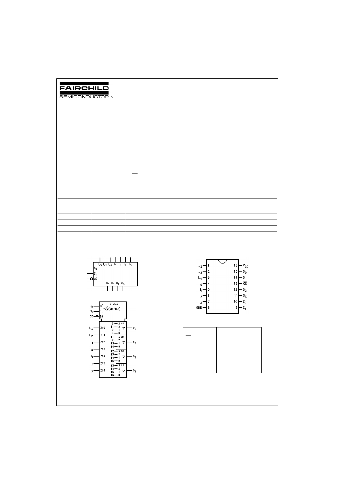
Logic Symbols
IEEE/IEC
Connection Diagram
Truth Table
H = HIGH Voltage Level
L = LOW Voltage Level
X = Immaterial
Z = High Impedance
Order Number Package Number Package Description
74F350SC M16A 16-Lead Small Outline Integrated Circuit (SOIC), JEDEC MS-012, 0.150 Narrow
74F350SJ M16D 16-Lead Small Outline Package (SOP), EIAJ TYPE II, 5.3mm Wide
74F350PC N16E 16-Lead Plastic Dual-In-Line Package (PDIP), JEDEC MS-001, 0.300 Wide
Inputs Outputs
OE
S1S0O0O1O2O
3
HXXZZZZ
LLLI
0I1I2I3
LLHI−1I0I1I
2
LHLI−2I−1I0I
1
LHHI−3I−2I−1I
0

www.fairchildsemi.com 2
74F350
Unit Loading/Fan Out
Functional Description
The 74F350 is operationally equivalent to a 4-input multiplexer with the inputs con nected so that the select code
causes successive one-bit shifts of the data word. This
internal connection makes it possible to perform shifts of 0,
1, 2 or 3 places on words of any length.
A 4-bit data word is introduced at the I
n
inputs and is
shifted according to the code applied to the select inputs
S
0
, S1. Outputs O0–O3 are 3-STATE, controlled by an
active LOW output en able (OE
). When OE is LOW, data
outputs will follow selected data inputs; when HIGH, the
data outputs will be forced to t he high impedance state.
This feature allows shifters to be cascaded on the same
output lines or to a co mmon bus. T he shift f uncti on can b e
logical, with zeros pulled in at either or both ends of the
shifting field; arith met i c, wh er e t he sign bit is repea ted du ring a shift down; or end around, where the data word forms
a continuous loop.
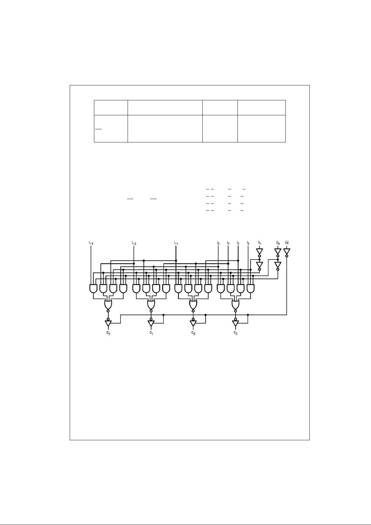
Logic Equations
O0 = S0S1I0 + S0S1I−1 + S0S1I−2 + S0S1I
−3
O1 = S0S1I1 + S0S1I0 + S0S1I−1 + S0S1I
−2
O2 = S0S1I2 + S0S1I1 + S0S1I0 + S0S1I
−1
O3 = S0S1I3 + S0S1I2 + S0S1I1 + S0S1I
0
Logic Diagram
Please note that this diagram is provided o nly f or t he understanding of lo gic operations and should not be used to estimate propagation delays.
Pin Names Description
U.L.
Input I
IH/IIL
HIGH/LOW
Output I
OH/IOL
S0, S
1
Select Inputs 1.0/2.0 20 µA/−1.2 mA
I
−3–I3
Data Inputs 1.0/2.0 20 µA/−1.2 mA
OE
Output Enable Input (Active LOW) 1.0/2.0 20 µA/−1.2 mA
O
0–O3
3-STATE Outputs 150/40 (33.3) −3 mA/24 mA (20 mA)

3 www.fairchildsemi.com
74F350
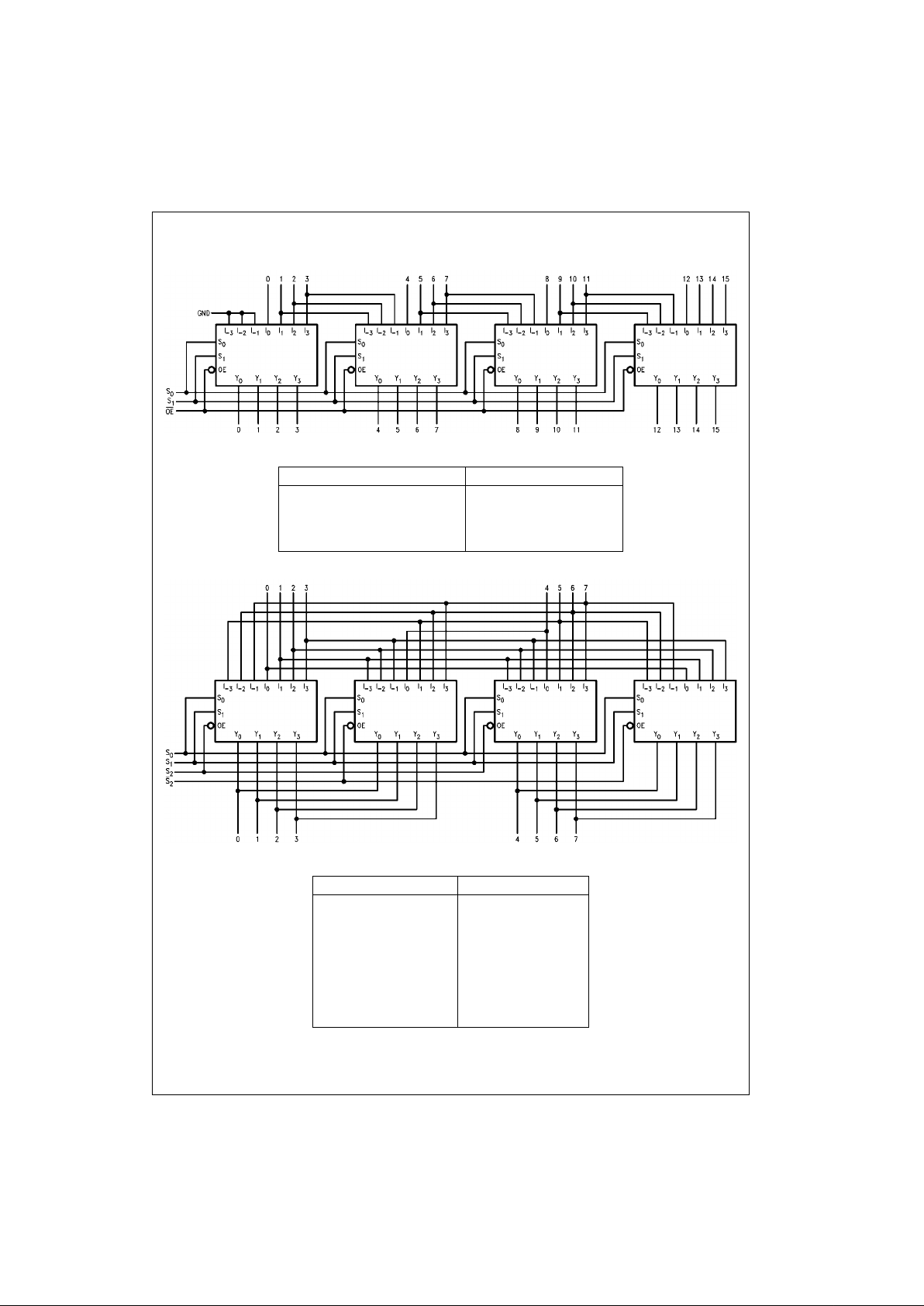
Applications
16-Bit Shift-Up 0 to 3 Places, Zero Backfill
Function Table
8-Bit End Around Shift 0 to 7 Places
Function Table
S
1
S
0
Shift Functi on
L L No Shift
L H Shift 1 Place
H L Shift 2 Places
H H Shift 3 Places
S
2
S
1
S
0
Shift Function
L L L No Shift
L L H Shift End Around 1
L H L Shift End Around 2
L H H Shift End Around 3
H L L Shift End Around 4
H L H Shift End Around 5
H H L Shift End Around 6
H H H Shift End Around 7
 Loading...