

Fairchild Semiconductor 74F283SJX, 74F283SCX, 74F283SC, 74F283PC Datasheet
© 1999 Fairchild Semiconductor Corporation DS009513 www.fairchildsemi.com
April 1988
Revised August 1999
74F283 4-Bit Binary Full Adder with Fast Carry
74F283
4-Bit Binary Full Adder with Fast Carry
General Description
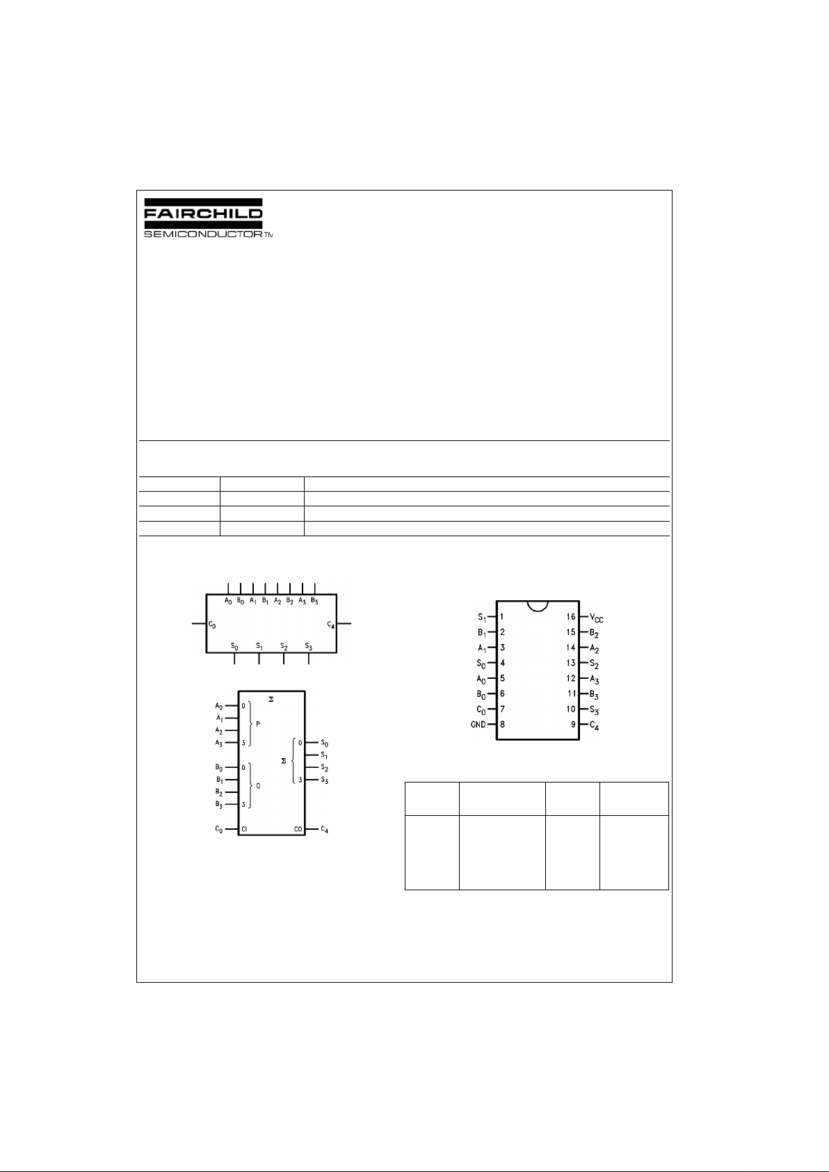
The 74F283 high -sp eed 4 -b i t b inar y full adder with in ter nal
carry lookahead accepts two 4-bit binary words (A
0–A3
,
B
0–B3
) and a Carry input (C0). It generates the binary Sum
outputs (S
0–S3
) and the Carry output (C4) from the most
significant bit. The 74F283 will operate with either active
HIGH or active LOW operands (positive or negative logic).
Ordering Code:
Devices also availab le in Tape and Reel. Specify by appending th e s uffix let t er “X” to the ordering code.
Logic Symbols
IEEE/IEC
Connection Diagram
Unit Loading/Fan Out
Order Number Package Number Package Description
74F283SC M16A 16-Lead Small Outline Integrated Circuit (SOIC), JEDEC MS-012, 0.150 Narrow
74F283SJ M16D 16-Lead Small Outline Package (SOP), EIAJ TYPE II, 5.3mm Wide
74F283PC N16E 16-Lead Plastic Dual-In-Line Package (PDIP), JEDEC MS-001, 0.300 Wide
Pin Names Description
U.L.
Input I
IH/IIL
HIGH/LOW
Output I
OH/IOL
A0–A3A Operand Inputs 1.0/2.0 20 µA/−1.2 mA
B
0–B3
B Operand Inputs 1.0/2.0 20 µA/−1.2 mA
C
0
Carry Input 1.0/1.0 20 µA/−0.6 mA
S
0–S3
Sum Outputs 50/33.3 −1 mA/20 mA
C
4
Carry Output 50/33.3 −1 mA/20 mA
www.fairchildsemi.com 2
74F283
Functional Description
The 74F283 adds two 4-bit binary words (A plus B) plus the
incoming Carry (C
0
). The binary sum a ppears on th e Sum
(S
0–S3
) and outgoing carry (C4) outputs. The binary weight
of the various inputs and output s is indicated by the subscript numbers, representing powers of two.
2
0
(A0 + B0 + C0) + 21 (A1 + B1)
+ 2
2
(A2 + B2) + 23 (A3 + B3)
= S
0
+ 2S1 + 4S2 + 8S3 + 16C
4
Where (+) = plus
Interchanging inpu ts of equal weight does not affect th e
operation. Thus C
0
, A0, B0 can be arbitrarily assigned to
pins 5, 6 and 7 for DIPS, and 7, 8 an d 9 for chip carrier
packages. Due to the symmetry of the binar y add functio n,
the 74F283 can be u sed either with all inputs and outputs
active HIGH (positive logic) or with all inputs and outputs
active LOW (negative logic). See Figure 1. Note that if C
0
is
not used it must be tied LOW for active HIGH logic or tied
HIGH for active LOW logic.
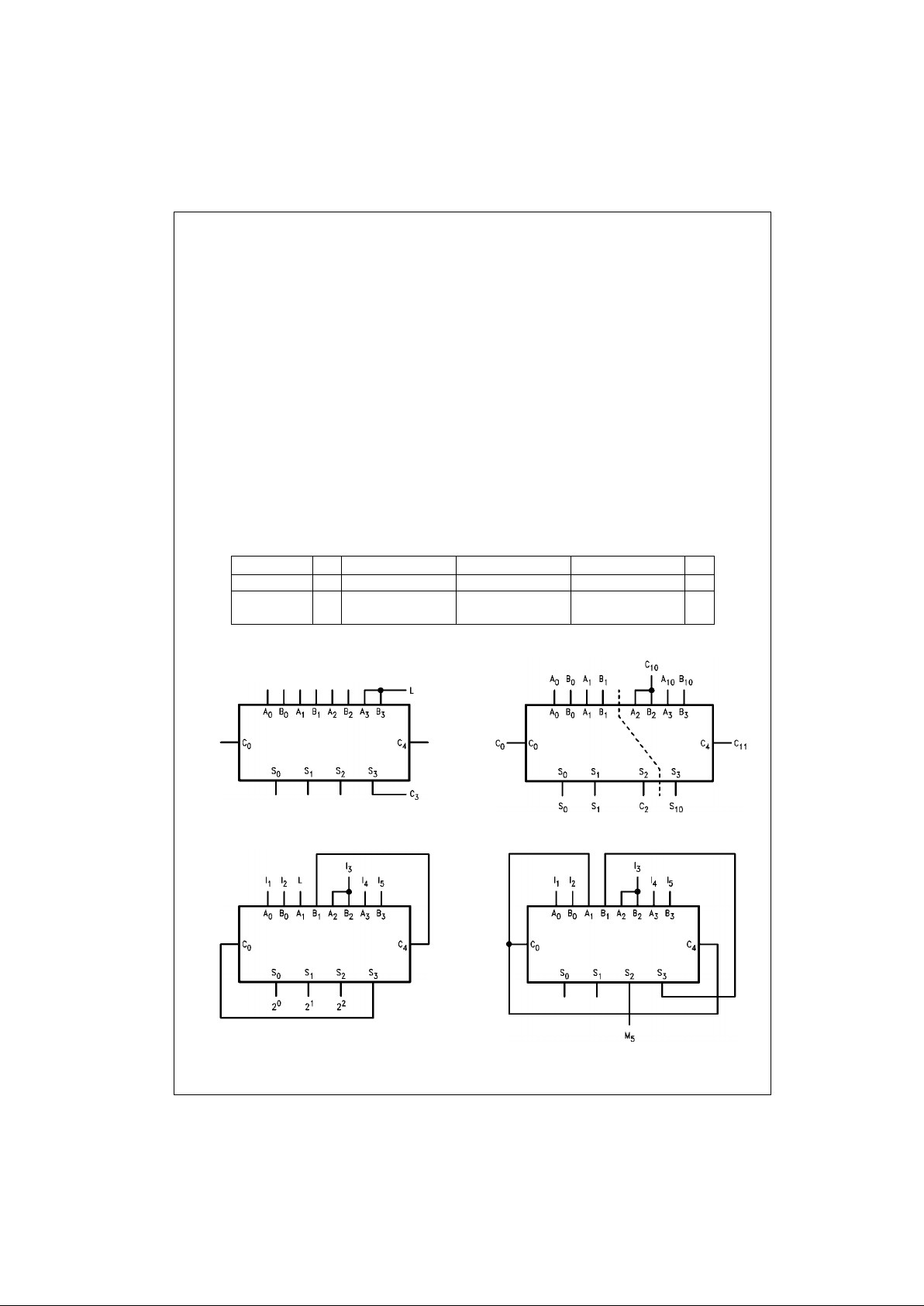
Due to pin limitations, the intermediate carries of the
74F283 are not brough t out for use as inputs or outputs.
However, other means can be us ed to effectively insert a
carry into, or bring a carry out from , an interm edia te stage.
Figure 2 shows ho w to m ake a 3 -bi t ad de r. Tying the operand inputs of the fourth adder (A
3
, B3) LOW makes S
3
dependent only on, and e qual to, the carry from the third
adder. Using somewhat the same principle, Figure 3 shows
a way of dividing the 74F283 into a 2- bit and a 1-b it add er.
The third stage adde r (A
2
, B2, S2) is used merely as a
means of getting a carry (C
10
) signal into the fourth stage
(via A
2
and B2) and bringing out the carr y from th e second
stage on S
2
. Note that as long as A2 and B2 are the same,
whether HIGH or LOW, they do not inf luen ce S
2
. Similarly,
when A
2
and B2 are the same the carry into th e th ird sta ge
does not influence the car ry o ut of the t hird stag e. F igur e 4
shows a method of implementing a 5-input encoder, where
the inputs are equally weighted. The outputs S
0
, S1 and S
2
present a binary number eq ual to the numbe r of inputs I1–
I
5
that are true. Figure 5 shows one method of imple ment-
ing a 5-input majority gate. When three or more of the
inputs I
1–I5
are true, the output M5 is true.
Active HIGH: 0 + 10 + 9 = 3 + 16 Active LOW: 1 + 5 + 6 = 12 + 0
FIGURE 1. Active HIGH versus Active LOW Interpretation
FIGURE 2. 3-Bit Adder FIGURE 3. 2-Bit and 1-Bit Adders
FIGURE 4. 5-Input Encoder FIGURE 5. 5-Input Majority Gate
C
0A0A1A2A3B0B1B2B3S0S1S2S3C4
Logic Levels L L H L H H L L H H H L L H
Active HIGH 00101100111001
Active LOW 11010011000110
 Loading...