

Fairchild Semiconductor 74F280SJX, 74F280SJ, 74F280SCX, 74F280SC, 74F280PC Datasheet
© 1999 Fairchild Semiconductor Corporation DS009512 www.fairchildsemi.com
April 1988
Revised August 1999
74F280 9-Bit Parity Generator/Checker
74F280
9-Bit Parity Generator/Checker
General Description
The F280 is a high-speed parity generator/checker that
accepts nine bits of input data and detects whether an
even or an odd number of t hese inputs is HIGH. If an even
number of inputs is HIGH, the Sum Even output is HIGH. If
an odd number is HIGH, the Sum Even output is LOW. The
Sum Odd output is t he complement of the Sum Even output.
Ordering Code:
Devices also availab le in Tape and Reel. Specify by appending th e s uffix let t er “X” to the ordering code.
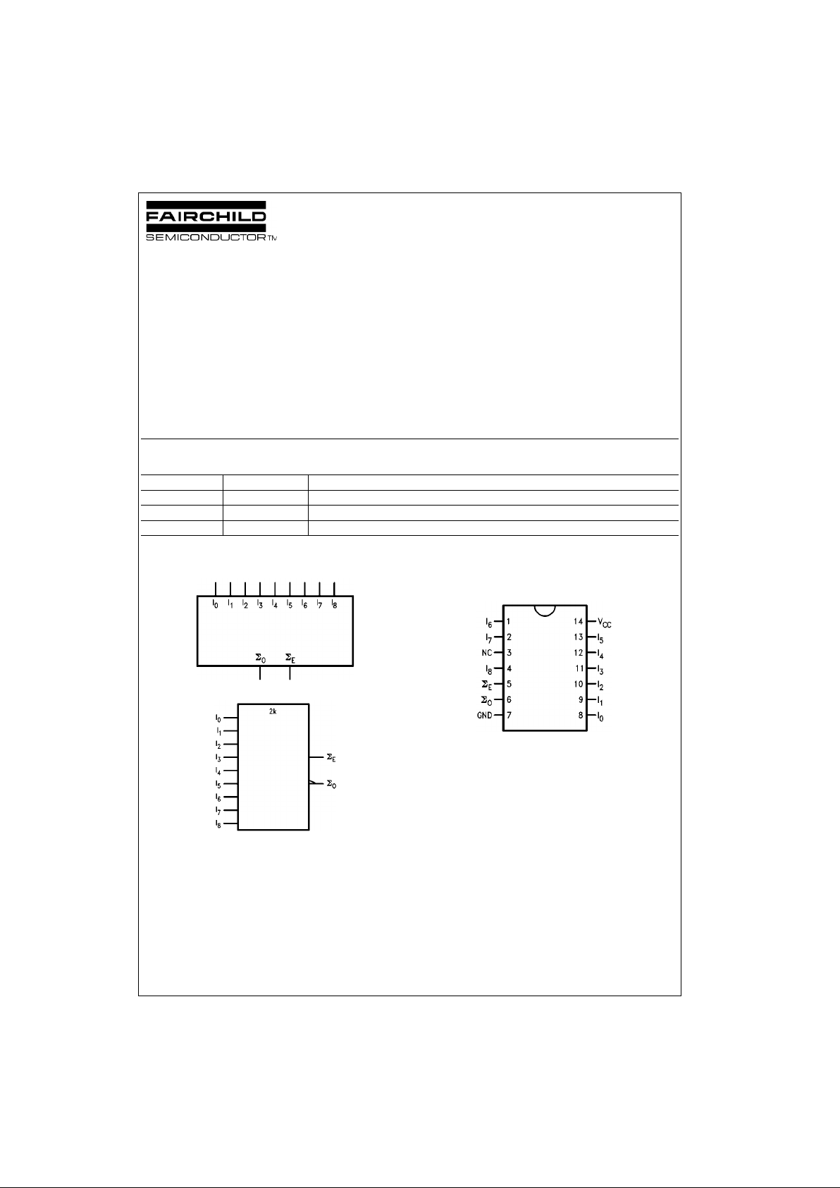
Logic Symbols
IEEE/IEC
Connection Diagram
Order Number Package Number Package Description
74F280SC M14A 14-Lead Small Outline Integrated Circuit (SOIC), JEDEC MS-120, 0.150 Narrow
74F280SJ M14D 14-Lead Small Outline Package (SOP), EIAJ TYPE II, 5.3mm Wide
74F280PC N14A 14-Lead Plastic Dual-In-Line Package (PDIP), JEDEC MS-001, 0.300 Wide
www.fairchildsemi.com 2
74F280
Unit Loading/Fan Out
Truth Table
H = HIGH Voltage Level
L = LOW Voltage Level
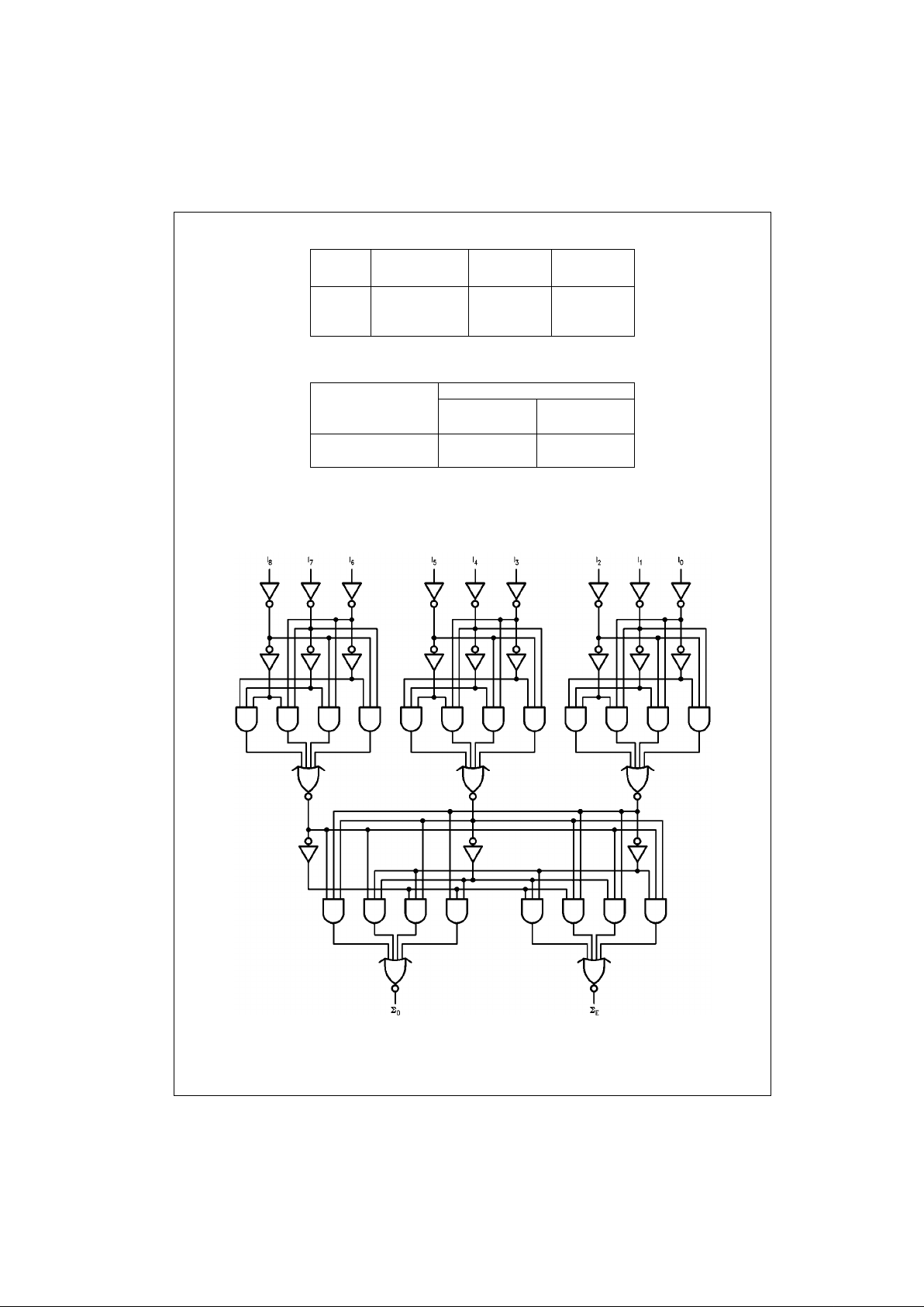
Logic Diagram
Please note that this diagram is provided o nly f or t he understanding of lo gic operations and should not be used to estimate propagation delays.
Pin Names Description
U.L.
Input I
IH/IIL
HIGH/LOW
Output I
OH/IOL
I0–I8Data Inputs 1.0/1.0 20 µA/−0.6 mA
∑
O
Odd Parity Output 50/33.3 −1 mA/20 mA
∑
E
Even Parity Output 50/33.3 −1 mA/20 mA
Number of Outputs
HIGH Inputs
∑ Even ∑ Odd
I
0–I8
0, 2, 4, 6, 8 H L
1, 3, 5, 7, 9 L H
 Loading...