Fairchild Semiconductor 74F251ASJ, 74F251ASCX, 74F251ASC, 74F251APC Datasheet

© 1999 Fairchild Semiconductor Corporation DS009504 www.fairchildsemi.com
April 1988
Revised August 1999
74F251A 8-Input Multiplexer with 3-STATE Outputs
74F251A
8-Input Multiplexer with 3-STATE Outputs
General Description
The 74F251A is a hig h-speed 8-i nput digital m ultiplexer. It
provides, in one package, the ability to select one bit of
data from up to eight sources. It can be used as a universal
function generator t o generate any logic function of four
variables. Both assertion and negation outputs are provided.
Features
■ Multifunctional capability
■ On-chip select logic decoding
■ Inverting and non-inverting 3-STATE outputs
Ordering Code:
Devices also availab le in Tape and Reel. Specify by appending th e s uffix let t er “X” to the ordering code.
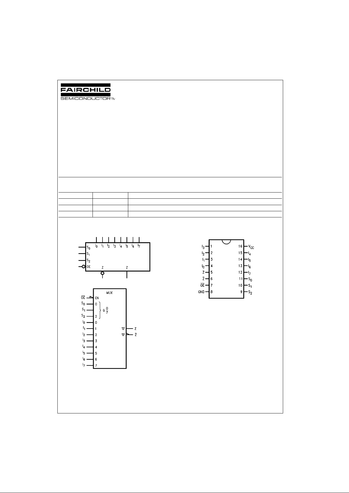
Logic Symbols
IEEE/IEC
Connection Diagram
Order Number Package Number Package Description
74F251ASC M16A 16-Lead Small Outline Integrated Circuit (SOIC), JEDEC MS-012, 0.150 Narrow
74F251ASJ M16D 16-Lead Small Outline Package (SOP), EIAJ TYPE II, 5.3mm Wide
74F251APC N16E 16-Lead Plastic Dual-In-Line Package (PDIP), JEDEC MS-001, 0.300 Wide

www.fairchildsemi.com 2
74F251A
Unit Loading/Fan Out
Functional Description
This device is a logical implementa tion of a single-pole, 8position switch with the switch position controlled by the
state of three Selec t inputs, S
0
, S1, S2. Both assertion and
negation outputs are provided. The Output Enable input
(OE
) is active LOW. When it is activated, the logic functi on
provided at the output is:
Z = OE
•(I0•S0•S1 •S2 + I1•S0•S 1•S2 +
I
2•S0•S1•S2
+ I3•S0•S1•S2 +
I
4•S0•S1•S2
+ I5•S0•S1•S2 +
I
6•S0•S1•S2
+ I7•S0•S1•S2)
When the Output Enabl e is HIGH, both outpu ts are in the
high impedance (High Z) state. This feature allows multiplexer expansion by tyin g the ou tput s of up to 128 dev ices
together. When the outputs of the 3-STATE devices are
tied together, all but one device must b e i n th e h igh im ped ance state to avo id high currents that would exc eed the
maximum ratings. The Output Enable signals should be
designed to ensure there is no over lap in the active L OW
portion of the enable voltages.
Tr uth Table
H = HIGH Voltage Level
L = LOW Voltage Level
X = Immaterial
Z = High Impedance
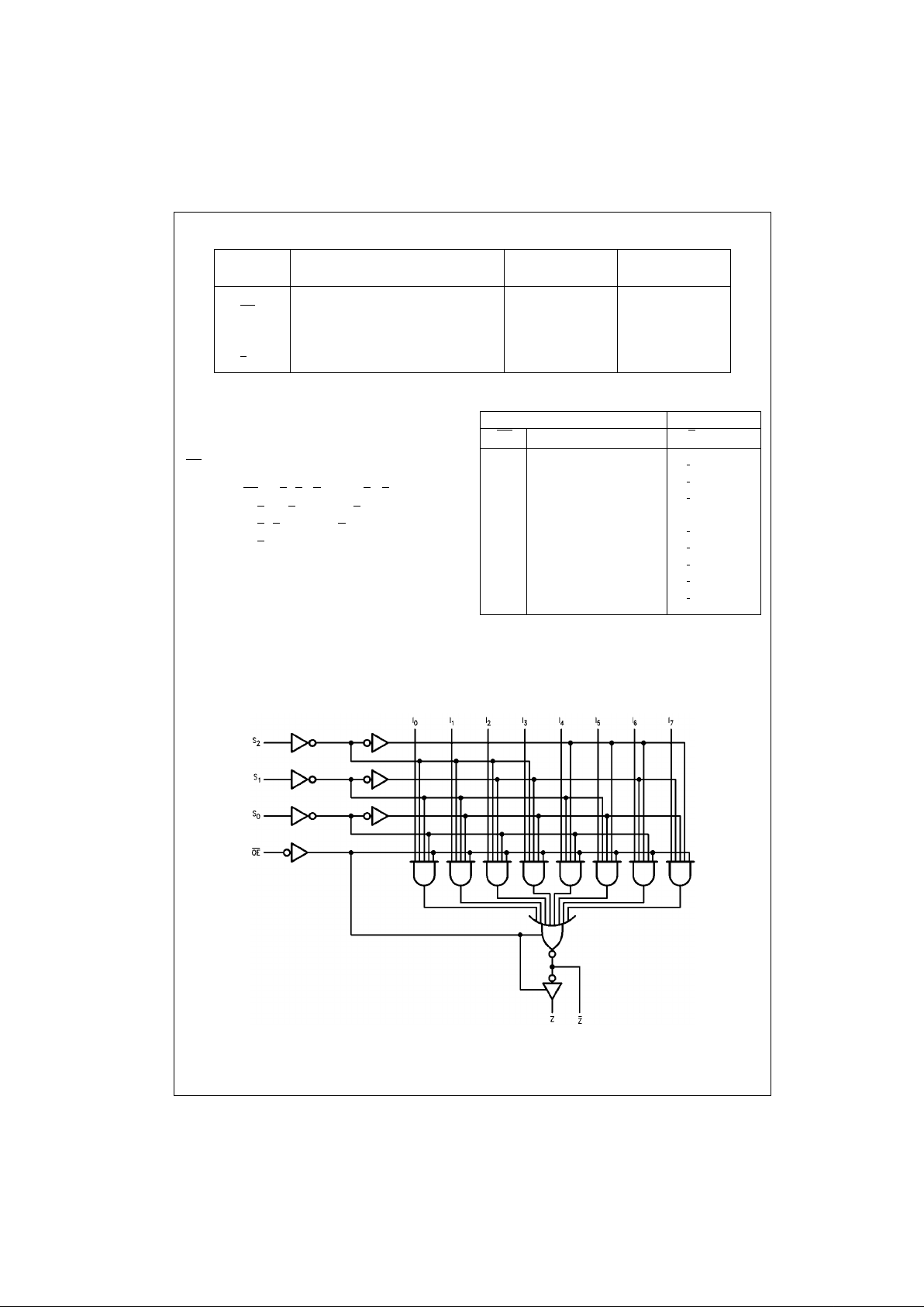
Logic Diagram
Please note that this diagram is provided o nly f or t he understanding of lo gic operations and should not be used to estimate propagation delays.
Pin Names Description
U.L.
Input I
IH/IIL
HIGH/LOW
Output I
OH/IOL
S0–S2Select Inputs 1.0/1.0 20 µA/−0.6 mA
OE
3-STATE Output Enable Input (Active LOW) 1.0/1.0 20 µA/−0.6 mA
I
0–I7
Multiplexer Inputs 1.0/1.0 20 µA/−0.6 mA
Z 3-STATE Multiplexer Output 150/40 (33.3) −3 mA/24 mA (20 mA)
Z
Complementary 3-STATE Multiplexer Output 150/40 (33.3) −3 mA/24 mA (20 mA)
Inputs Outputs
OE
S
2
S
1
S
0
Z Z
HXXXZZ
LLLLI
0
I
0
LLLHI1I
1
LLHLI2I
2
LLHHI3I
3
LHLLI4I
4
LHLHI5I
5
LHHLI6I
6
LHHHI7I
7
 Loading...