

Fairchild Semiconductor 74F245MTCX, 74F245MTC, 74F245MSAX, 74F245MSA, 74F245CW Datasheet
...
April 1988
Revised April 1999
74F245 Octal Bidirectional Transceiver with 3-STATE Outputs
© 1999 Fairchild Semiconductor Corporation DS009503.prf www.fairchildsemi.com
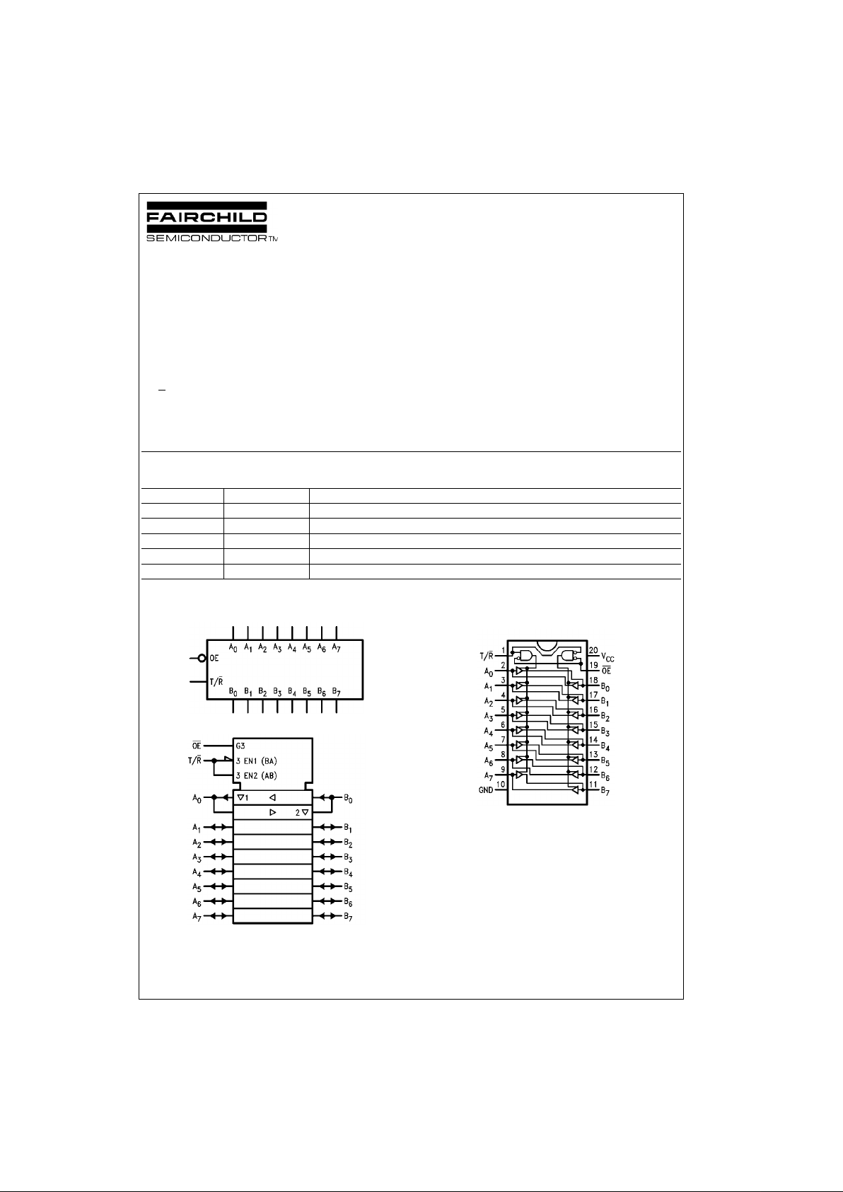
74F245
Octal Bidirectional Transceiver with 3-STATE Outputs
General Description
The 74F245 contains ei ght non-in verting b idirection al buffers with 3-STATE outputs and is intended for bus-ori ented
applications. Current sinking capability is 24 mA at the A
Ports and 64 mA at the B Ports. The Transmit/Receive
(T/R
) input determines the direction of data flow through
the bidirectional transceiver. Transmit (active HIGH)
enables data from A Ports to B Ports; Receive (active
LOW) enables data from B Ports to A Ports. The Outp ut
Enable input, when HIGH, disa bles both A a nd B Por ts by
placing them in a High Z condition.
Features
■ Non-inverting buffers
■ Bidirectional data path
■ A outputs sink 24 mA
■ B outputs sink 64 mA
Ordering Code:
Devices also availab le in Tape and Reel. Specify by appending th e s uffix let t er “X” to the ordering cod e.
Logic Symbols
IEEE/IEC
Connection Diagram
Order Number Package Number Package Description
74F245SC M20B 20-Lead Small Outline Integrated Circuit (SOIC), JEDEC MS-013, 0.300 Wide
74F245SJ M20D 20-Lead Small Outline Package (SOP), EIAJ TYPE II, 5.3mm Wide
74F245MSA MSA20 20-Lead Shrink Small Outline Package (SSOP), EIAJ TYPE II, 5.3mm Wide
74F245MTC MTC20 20-Lead Thin Shrink Small Outline Package (TSSOP), JEDEC MO-153, 4.4mm Wide
74F245PC N20A 20-Lead Plastic Dual-In-Line Package (PDIP), JEDEC MS-001, 0.300 Wide
www.fairchildsemi.com 2
74F245
Unit Loading/Fan Out
Truth Table
H = HIGH Voltage Level
L = LOW Voltage Level
X = Immaterial
Pin Names Description
U.L.
Input I
IH/IIL
HIGH/LOW
Output I
OH/IOL
OE Output Enable Input (Active LOW) 1.0/2.0 20 µA/−1.2 mA
T/R
Transmit/Receive Input 1.0/2.0 20 µA/−1.2 mA
A
0–A7
Side A Inputs or 3.5/1.083 70 µA/−0.65 mA
3-STATE Outputs 150/40(38.3) −3 mA/24 mA (20 mA)
B
0–B7
Side B Inputs or 3.5/1.083 70 µA/−0.65 mA
3-STATE Outputs 600/106.6(80) −12 mA/64 mA (48 mA)
Inputs
Output
OE
T/R
L L Bus B Data to Bus A
L H Bus A Data to Bus B
H X High Z State
3 www.fairchildsemi.com
74F245
Absolute Maximum Ratings(Note 1) Recommended Operating
Conditions
Note 1: Absolute maximum ratings are values beyon d which the device
may be damaged or have its useful life impaired . Functional operation
under these condit ions is not implied.
Note 2: Either voltage limit or curren t limit is sufficient to protect in puts.
DC Electrical Characteristics
Storage Temperature −65°C to +150°C
Ambient Temperature under Bias −55°C to +125°C
Junction Temperature under Bias −55°C to +150°C
V
CC
Pin Potential to Ground Pin −0.5V to +7.0V
Input Voltage (Note 2) −0.5V to +7.0V
Input Current (Note 2) −30 mA to +5.0 mA
Voltage Applied to Output
in HIGH State (with V
CC
= 0V)
Standard Output −0.5V to V
CC
3-STATE Output −0.5V to +5.5V
Current Applied to Output
in LOW State (Max) twice the r ated I
OL
(mA)
ESD Last Passing Voltage (Min) 4000V
Free Air Ambi ent Temperature 0°C to +70°C
Supply Voltage +4.5V to +5.5V
Symbol Parameter Min Typ Max Units
V
CC
Conditions
V
IH
Input HIGH Voltage 2.0 V Recognized as a HIGH Signal
V
IL
Input LOW Voltage 0.8 V Recognized as a LOW Signal
V
CD
Input Clamp Diode Voltage −1.2 V Min IIN = −18 mA
V
OH
Output HIGH Voltage 10% V
CC
2.4 V Min IOH = −3 mA (An)
10% V
CC
2.0 IOH = −15 mA (Bn)
5% V
CC
2.7 IOH = −3 mA (An)
V
OL
Output LOW Voltage 10% V
CC
0.5 V Min IOL = 24 mA (An)
10% V
CC
0.55 IOL = 64 mA (Bn)
I
IH
Input HIGH Current 5.0 µAMaxVIN = 2.7V
I
BVI
Input HIGH Current Breakdown Test 7.0
µAMax
VIN = 7.0V (OE, T/R)
I
BVIT
Input HIGH Current Breakdown (I/O) 0.5 mA Max VIN = 5.5 V (An, Bn)
I
CEX
Output HIGH Leakage Current 50 µAMaxV
OUT
= VCC (An, Bn)
V
ID
Input Leakage 4.75 V 0.0 IID = 1.9 µA
Test All Other Pins Grounded
I
OD
Output Leakage 3.75 µA0.0V
IOD
= 150 mV
Circuit Current All Other Pins Grounded
I
IL
Input LOW Current −1.2 mA Max
VIN = 0.5V (T/R, OE)
IIH + I
OZH
Output Leakage Current 70 µAMaxV
OUT
= 2.7V (An, Bn)
IIL + I
OZL
Output Leakage Current −650 µAMaxV
OUT
= 0.5V (An, Bn)
I
OS
Output Short-Circuit Current −60 −150 mA Max V
OUT
= 0V (An)
−100 −225 V
OUT
= 0V (Bn)
I
ZZ
Bus Drainage Test 500 µA0.0VV
OUT
= 5.25V(An, Bn)
I
CCH
Power Supply Current 70 90 mA Max VO = HIGH
I
CCL
Power Supply Current 95 120 mA Max VO = LOW
I
CCZ
Power Supply Current 85 110 mA Max VO = HIGH Z
 Loading...