

Fairchild Semiconductor 74F243SCX, 74F243SC Datasheet
74F243
Quad Bus Tr ansceiver with 3-STAT E Outputs
74F243 Quad Bus Transceiver with 3-STATE Outputs
April 1988
Revised July 1999
General Description
The 74F243 is a quad bus transmitter/receiver designed for
4-line asynchronous 2-wa y data communica tions between
data busses.
Features
■ 2-Way asynchronous data bus communication
■ Input cl amp diodes limit high-speed term ination effects
Ordering Code:
Order Code Package Number Package Description
74F243SC M14A 14-Lead Small Outline Integrated Circuit (SOIC), JEDEC MS-120, 0.150 Narrow
Devices also availab le in Tape and Reel. Specify by appending th e s uffix let t er “X” to the ordering cod e.
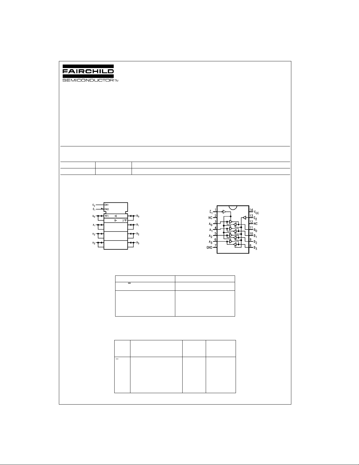
Logic Symbol
IEEE/IEC
Connection Diagram
Truth Table
Inputs Inputs/Outputs
E
L L Input B = A
LHN/AN/A
HLZZ
H = HIGH Voltage Level Z = High Impedance
L = LOW Voltage Level N/A = Not Allowed
HHA = B Input
1
E
2
A
n
B
n
Unit Loading/Fan Out
Pin
Names
E
1
E
2
, BnInputs 3.5/2.67 70 µA/−1.6 mA
A
n
© 1999 Fairchild Semiconductor Corporation DS009502 www.fairchildsemi.com
Description
Enable Input (Active LOW) 1.0/1.67 20 µA/−1 mA
Enable Input (Active HIGH) 1.0/1.67 20 µA/−1 mA
Outputs 600/106.6
U.L.
HIGH/LOW
(80)
Input I
IH/IIL
Output IOH/I
−12 mA/64 mA
(48 mA)
OL
Absolute Maximum Ratings(Note 1) Recommended Operating
Storage Temperature −65°C to +150°C
74F243
Ambient Temperature under Bias −55°C to +125°C
Junction Temperature under Bias −55°C to +150°C
Pin Potential to Ground Pin −0.5V to +7.0V
V
CC
Input Voltage (Note 2) −0.5V to +7.0V
Input Current (Note 2) −30 mA to +5.0 mA
Voltage Applied to Output
in HIGH State (with V
CC
= 0V)
Standard Output −0.5V to V
3-STATE Output −0.5V to +5.5V
Current Applied to Output
in LOW State (Max) twice the rated I
ESD Last Passing Voltage (Min) 4000V
OL
Conditions
Free Air Ambient Temperature 0°C to +70°C
Supply Voltage +4.5V to +5.5V
Note 1: Absolute maximum ratings are values beyond which the device
CC
may be damaged or have its useful life impaired. Functional operation
under these conditi ons is not implied.
Note 2: Either voltage limit or curren t limit is sufficient to protect in put s .
(mA)
DC Electrical Characteristics
Symbol Parameter Min Typ Max Units
V
IH
V
IL
V
CD
V
OH
V
OL
I
IH
I
BVI
I
BVIT
I
CEX
V
ID
I
OD
I
IL
IIH + I
IIL + I
I
OS
I
CCH
I
CCL
I
CCZ
Input HIGH Voltage 2.0 V Recognized as a HIGH Signal
Input LOW Voltage 0.8 V Recognized as a LOW Signal
Input Clamp Diode Voltage −1.2 V Min IIN = −18 mA
Output HIGH 10% V
Voltage 10% V
5% V
Output LOW 10% V
Voltage
Input HIGH
Current
Input HIGH Current
Breakdown Test
Input HIGH Current
Breakdown (I/O)
Output HIGH
Leakage Current
Input Leakage
Test All Other Pins Grounded
Output Leakage
Circuit Current All Other Pins Grounded
2.4
CC
2.0 IOH = −15 mA (An, Bn)
CC
2.7 IOH = −3 mA (An, Bn)
CC
CC
0.55 V Min IOL = 64 mA (An, Bn)
5.0 µAMaxVIN = 2.7V
7.0 µAMaxVIN = 7.0V (E1, E2)
0.5 mA Max VIN = 5.5V (An, Bn)
50 µAMaxV
4.75 V 0.0
3.75 µA0.0
Input LOW Current −1.0 mA Max VIN = 0.5V (E1, E2)
Output Leakage Current 70 µAMaxV
OZH
Output Leakage Current −1.6 mA Max V
OZL
Output Short-Circuit Current −100 −225 mA Max V
Power Supply Current 64 80 mA Max VO = HIGH
Power Supply Current 64 90 mA Max VO = LOW
Power Supply Current 71 90 mA Max VO = HIGH Z
V
CC
IOH = −3 mA (An, Bn)
VMin
IID = 1.9 µA
V
Conditions
= V
OUT
CC
= 150 mV
IOD
= 2.7V (An, Bn)
OUT
= 0.5V (An, Bn)
OUT
= 0V (An, Bn)
OUT
www.fairchildsemi.com 2
 Loading...