

Fairchild Semiconductor 74F240SJ, 74F240SCX, 74F240SC, 74F240PC, 74F240SJX Datasheet
© 1999 Fairchild Semiconductor Corporation DS009501 www.fairchildsemi.com
April 1988
Revised July 1999
74F240 • 74F241 • 74F244 Octal Buffers/Line Drivers with 3-STATE Outputs
74F240 • 74F241 • 74F244
Octal Buffers/Line Drivers with 3-STATE Outputs
General Description
The 74F240, 74F241 and 74F244 are octal buffers and line
drivers designed to be employ ed as memory and address
drivers, clock drivers a nd bus-oriented transmitters/ receivers which provide improved PC and board density.
Features
■ 3-STATE outputs drive bus lines or buffer memory
address registers
■ Outputs sink 64 mA (48 mA mil)
■ 12 mA source current
■ Input clamp diodes limit high-speed termination effects
Ordering Code:
Devices also availab le in Tape and Reel. Specify by appending th e s uffix let t er “X” to the ordering code.
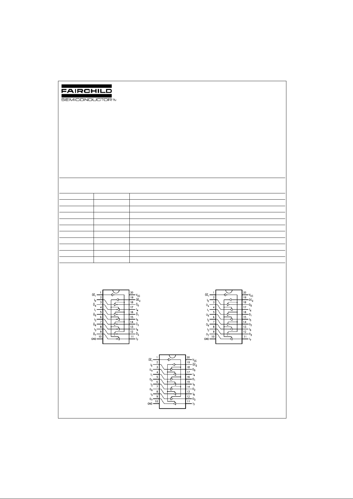
Connection Diagrams
74F240 74F241
74F244
Order Code Package Number Package Description
74F240SC M20B 20-Lead Small Outline Integrated Circuit (SOIC), JEDEC MS-013, 0.300 Wide
74F240SJ M20D 20-Lead Small Outline Package (SOP), EIAJ TYPE II, 5.3mm Wide
74F240PC N20A 20-Lead Plastic Dual-In-Line Package (PDIP), JEDEC MS-001, 0.300 Wide
74F241SC M20B 20-Lead Small Outline Integrated Circuit (SOIC), JEDEC MS-013, 0.300 Wide
74F241SJ M20D 20-Lead Small Outline Package (SOP), EIAJ TYPE II, 5.3mm Wide
74F241PC N20A 20-Lead Plastic Dual-In-Line Package (PDIP), JEDEC MS-001, 0.300 Wide
74F244SC M20B 20-Lead Small Outline Integrated Circuit (SOIC), JEDEC MS-013, 0.300 Wide
74F244SJ M20D 20-Lead Small Outline Package (SOP), EIAJ TYPE II, 5.3mm Wide
74F244MSA MSA20 20-Lead Shrink Small Outline Package (SSOP), EIAJ TYPE II, 5.3mm Wide
74F244PC N20A 20-Lead Plastic Dual-In-Line Package (PDIP), JEDEC MS-001, 0.300 Wide
www.fairchildsemi.com 2
74F240 • 74F241 • 74F244
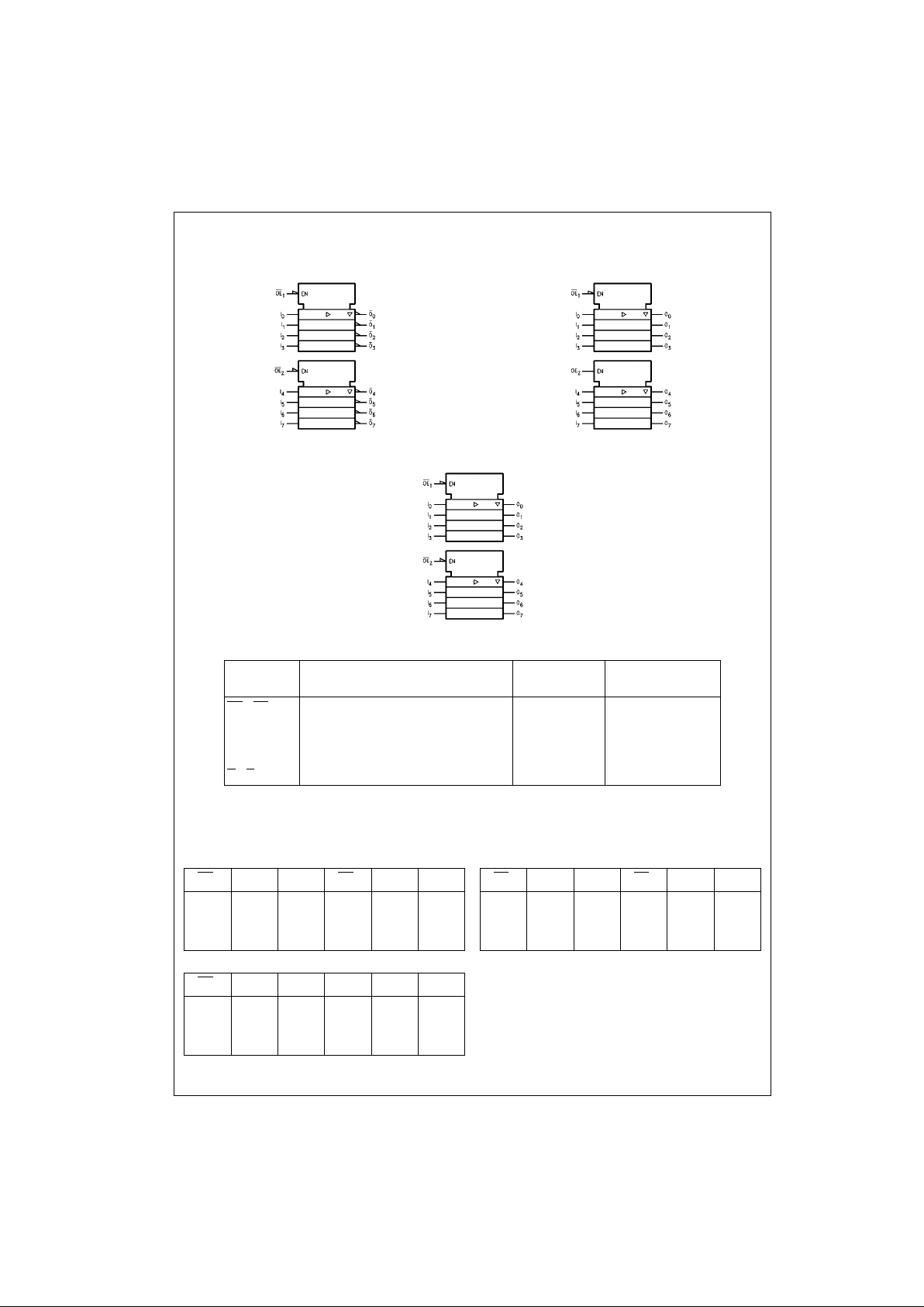
Logic Symbols
IEEE/IEC
74F240
IEEE/IEC
74F241
IEEE/IEC
74F244
Unit Loading/Fan Out
Note 1: Worst-case 74F240 enabled; 74F 241, 74F244 disabled
Truth Tables
74F240
74F241
74F244
H = HIGH Voltage Level
L = LOW Voltage Level
X = Immaterial
Z = High Impedance
Pin Names Description
U.L.
Input I
IH/IIL
HIGH/LOW
Output I
OH/IOL
OE1, OE
2
3-STATE Output Enable Input (Active LOW) 1.0/1.667 20 µA/−1 mA
OE
2
3-STATE Output Enable Input (Active HIGH) 1.0/1.667 20 µA/−1 mA
I
0–I7
Inputs (74F240) 1.0/1.667 (Note 1) 20 µA/−1 mA
I
0–I7
Inputs (74F241, 74F244) 1.0/2.667 (Note 1) 20 µA/−1.6 mA
O
0–O7
, O0–O7Outputs 600/106.6 (80) −12 mA/64 mA (48 mA)
OE
1
D
1n
O
1n
OE
2
D
2n
O
2n
HXZHXZ
LHLLHL
LLHLLH
OE
1
D
1n
O
1n
OE
2
D
2n
O
2n
HXZLXZ
LHHHHH
LLLHLL
OE
1
D
1n
O
1n
OE
2
D
2n
O
2n
HXZHXZ
LHHLHH
LLLLLL
3 www.fairchildsemi.com
74F240 • 74F241 • 74F244
Absolute Maximum Ratings(Note 2) Recommended Operating
Conditions
Note 2: Absolute maximum ratings are values beyon d which the device
may be damaged or have its useful life impaired . Functional operation
under these condit ions is not implied.
Note 3: Either voltage limit or curren t limit is sufficient to protect in puts.
DC Electrical Characteristics
Storage Temperature −65°C to +150°C
Ambient Temperature under Bias −55°C to +125°C
Junction Temperature under Bias −55°C to +150°C
V
CC
Pin Potential to Ground Pin −0.5V to +7.0V
Input Voltage (Note 3) −0.5V to +7.0V
Input Current (Note 3) −30 mA to +5.0 mA
Voltage Applied to Output
in HIGH State (with V
CC
= 0V)
Standard Output −0.5V to V
CC
3-STATE Output −0.5V to +5.5V
Current Applied to Output
in LOW State (Max) twice the r ated I
OL
(mA)
ESD Last Passing Voltage (Min) 4000V
Free Air Ambi ent Temperature 0°C to +70°C
Supply Voltage +4.5V to +5.5V
Symbol Parameter Min Typ Max Units
V
CC
Conditions
V
IH
Input HIGH Voltage 2.0 V Recognized as a HIGH Signal
V
IL
Input LOW Voltage 0.8 V Recognized as a LOW Signal
V
CD
Input Clamp Diode Voltage −1.2 V Min IIN = −18 mA
V
OH
Output HIGH 10% VCC2.4
VMin
IOH = −3 mA
Voltage 10% VCC2.0 IOH = −15 mA
5% VCC2.7 IOH = −3 mA
V
OL
Output LOW 10% V
CC
0.55 V Min IOL = 64 mA
Voltage
I
IH
Input HIGH
5.0 µAMaxVIN = 2.7V
Current
I
BVI
Input HIGH Current
7.0 µAMaxVIN = 7.0V
Breakdown Test
I
CEX
Output HIGH
50 µAMaxV
OUT
= V
CC
Leakage Current
V
ID
Input Leakage
4.75 V 0.0
IID = 1.9 µA
Test All Other Pins Grounded
I
OD
Output Leakage
3.75 µA0.0
V
IOD
= 150 mV
Circuit Current All Other Pins Grounded
I
IL
Input LOW Current −1.0
mA Max
VIN = 0.5V (OE1, OE2, OE2, Dn 74F240))
−1.6 VIN = 0.5V (Dn (74F241, 74F244))
I
OZH
Output Leakage Current 50 µAMaxV
OUT
= 2.7V
I
OZL
Output Leakage Current −50 µAMaxV
OUT
= 0.5V
I
OS
Output Short-Circuit Current −100 −225 mA Max V
OUT
= 0V
I
ZZ
Bus Drainage Test 500 µA0.0VV
OUT
= 5.25V
I
CCH
Power Supply Current (74F240) 19 29 mA Max VO = HIGH
I
CCL
Power Supply Current (74F240) 50 75 mA Max VO = LOW
I
CCZ
Power Supply Current (74F240) 42 63 mA Max VO = HIGH Z
I
CCH
Power Supply Current
40 60 mA Max VO = HIGH
(74F241, 74F244)
I
CCL
Power Supply Current
60 90 mA Max VO = LOW
(74F241, 74F244)
I
CCZ
Power Supply Current
60 90 mA Max
VO = HIGH Z
(74F241, 74F244)
 Loading...