

Fairchild Semiconductor 74F193SJ, 74F193SCX, 74F193SC, 74F193PC Datasheet

© 1999 Fairchild Semiconductor Corporation DS009497 www.fairchildsemi.com
April 1988
Revised July 1999
74F193 Up/Down Binary Counter with Separate Up/Down Clocks
74F193
Up/Down Binary Counter with Separate Up/Down Clocks
General Description
The 74F193 is an up/down modulo-16 binary counter. Separate Count Up and Count D own Clocks are used, an d in
either counting mode the circuits operate synchronously.
The outputs change stat e synchronousl y with the LO W-toHIGH transitions on the clock inputs. Separate Terminal
Count Up and Terminal Count Down outputs are provid ed
that are used as the clock s for subsequen t stages withou t
extra logic, thus simplifying multi-stage counter designs.
Individual preset inputs allow the circuit to be used as a
programmable counter. Both the Parallel Load (PL
) and the
Master Reset (MR) inputs asynchronously override the
clocks.
Ordering Code:
Devices also availab le in Tape and Reel. Specify by appending su ffix let te r “X” to the ordering code.
Logic Symbols
IEEE/IEC
Connection Diagram
Order Number Package Number Package Description
74F193SC M16A 16-Lead Small Outline Integrated Circuit (SOIC), JEDEC MS-012, 0.150” Narrow Body
74F193SJ M16D 16-Lead Small Outline Package (SOP), EIAJ TYPE II, 5.3mm Wide
74F193PC N16E 16-Lead Plastic Dual-In-Line Package (PDIP), JEDEC MS-001, 0.300” Wide
www.fairchildsemi.com 2
74F193
Unit Loading/Fan Out
Functional Description
The 74F193 is a 4-bit binary synchronous up/down (reversible) counter. It contains four edge-triggered flip-flops, with
internal gating and steering logic to provide master reset,
individual preset, count up and count down operations.
A LOW-to-HIGH transition on the CP inpu t to each flip-flo p
causes the output to change state. Synchronous switching,
as opposed to ripp le counting, is achieved by dr iving the
steering gates o f all st ages from a commo n Count U p line
and a common Count Down line, thereby causing a ll state
changes to be initiated simultaneously. A LOW-to-HIGH
transition on the Count Up input will adva nce the count by
one; a similar transition on the Count Down input will
decrease the count by one. While counti ng with one cl ock
input, the other sh ould be held HIGH, as indica ted in the
Function Table.
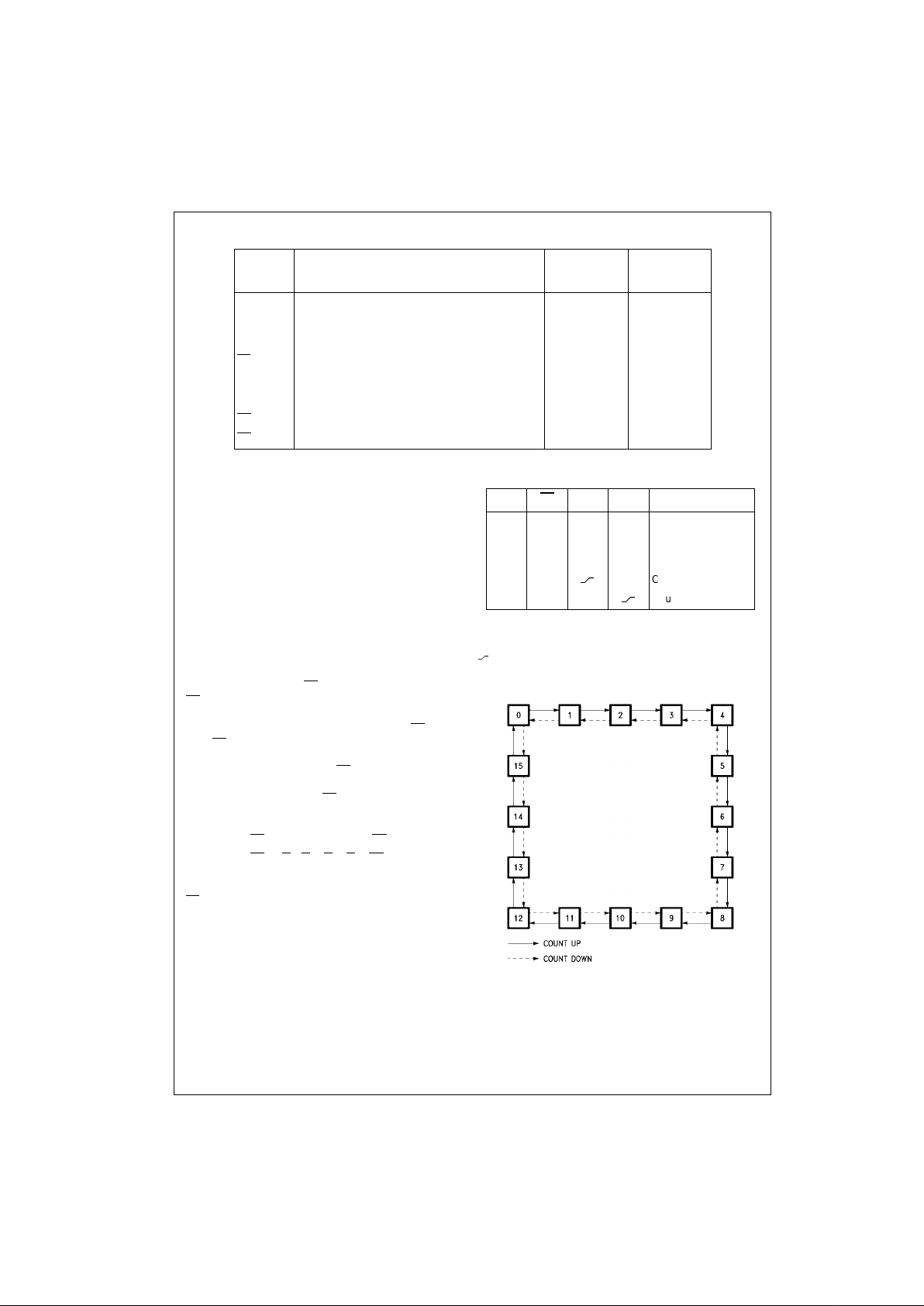
The Terminal Count Up (TC
U
) and Terminal Count Down
(TC
D
) outputs are normally HIGH. When the circuit has
reached the maximum count state 15, the next HIGH-toLOW transition of the Count Up Clock will cause TC
U
to go
LOW. TC
U
will stay LOW until CPU goes HIGH agai n, th us
effectively repeating the Cou nt Up Clock, but delayed by
two gate delays. Similarly, the TC
D
output will go LOW
when the circuit is in the zero state and the Count Down
Clock goes LOW. Since the TC
outputs repeat the cl ock
waveforms, they can be used as the cl ock input sign als to
the next higher order circuit in a multistage counter.
TC
U
= Q0 • Q1 • Q2 • Q3 • CP
U
TCD = Q0• Q1 • Q2 • Q3 • CP
D
The 74F193 has an asynchronous parallel load capability
permitting the counter to be preset. When the Parallel Load
(PL
) and the Master Reset ( MR) inputs ar e LOW, informa-
tion present on the Parallel Data input (P
0–P3
) is loaded
into the counter and appears on the outputs regardless of
the conditions of the clock inpu ts. A HIGH signal on the
Master Reset input will d isable the preset gates, ove rride
both clock inputs, and latch each Q output in the LOW
state. If one of t he clock inp uts is LOW du ring and aft er a
reset or load operation, the next LOW-to-HIGH transition of
that clock will be interpreted as a legitimate signal and will
be counted.
Function Table
H = HIGH Voltage Level
L = LOW Voltage Level
X = Immaterial
= LOW-to-HIGH Clock Transition
State Diagram
Pin Names Description
U.L.
Input I
IH/IIL
HIGH/LOW
Output I
OH/IOL
CP
U
Count Up Clock Input (Active Rising Edge) 1.0/3.0 20 µA/−1.8 mA
CP
D
Count Down Clock Input (Active Rising Edge) 1.0/3.0 20 µA/−1.8 mA
MR Asynchronous Master Reset Input (Active HIGH) 1.0/1.0 20 µA/−0.6 mA
PL
Asynchronous Parallel Load Input (Active LOW) 1.0/1.0 20 µA/−0.6 mA
P
0–P3
Parallel Data Inputs 1.0/1.0 20 µA/−0.6 mA
Q
0–Q3
Flip-Flop Outputs 50/33.3 −1 mA/20 mA
TC
D
Terminal Count Down (Borrow) Output (Active LOW) 50/33.3 −1 mA/20 mA
TC
U
Terminal Count Up (Carry) Output (Active LOW) 50/33.3 −1 mA/20 mA
MR PL
CPUCP
D
Mode
H X X X Reset (Asyn.)
L L X X Preset (Asyn.)
L H H H No Change
LH
H Count Up
LHH
Count Down
3 www.fairchildsemi.com
74F193
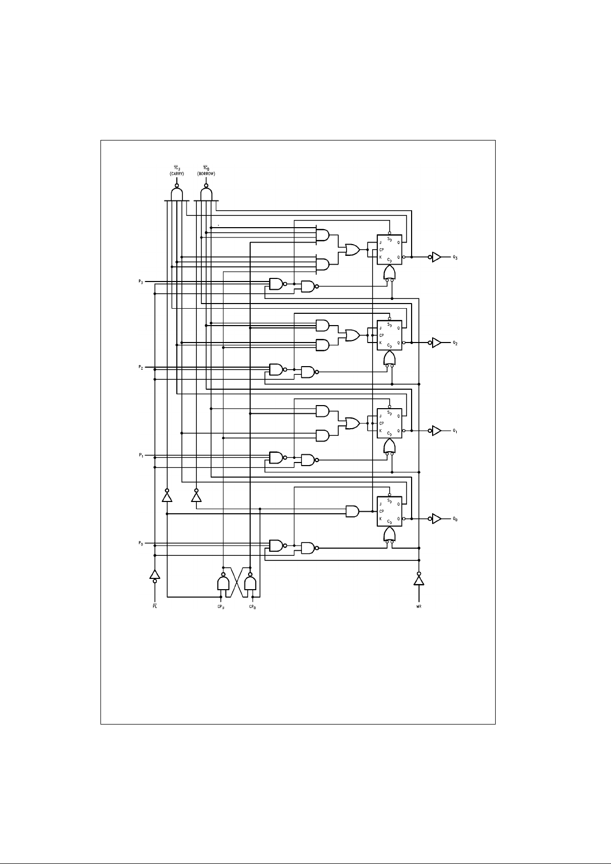
Logic Diagram
Please note that this d iagram is provided only f or t he understanding of lo gic operations and should not be used to estimat e propagation delays.
 Loading...