

Datasheet 74F148CW, 74F148SJX, 74F148SJ, 74F148SCX, 74F148SC Datasheet (Fairchild Semiconductor)
...Page 1
© 1999 Fairchild Semiconductor Corporation DS009480 www.fairchildsemi.com
April 1988
Revised July 1999
74F148 8-Line to 3-Line Priority Encoder
74F148
8-Line to 3-Line Priority Encoder
General Description
The F148 provide s three bits of bina ry code d output representing the position o f the highest order active input, along
with an out p ut i n dic a t ing t he p re s enc e o f an y ac t iv e i nput . I t
is easily expanded via i nput and o utput enable s to p rovi de
priority encoding over many bit s.
Features
■ Encodes eight data lines in priority
■ Provides 3-bit binary priority code
■ Input enable capability
■ Signals when data is present on any input
■ Cascadable for priority encoding of n bits
Ordering Code:
Devices also availab le in Tape and Reel. Specify by appending th e s uffix let t er “X” to the ordering code.
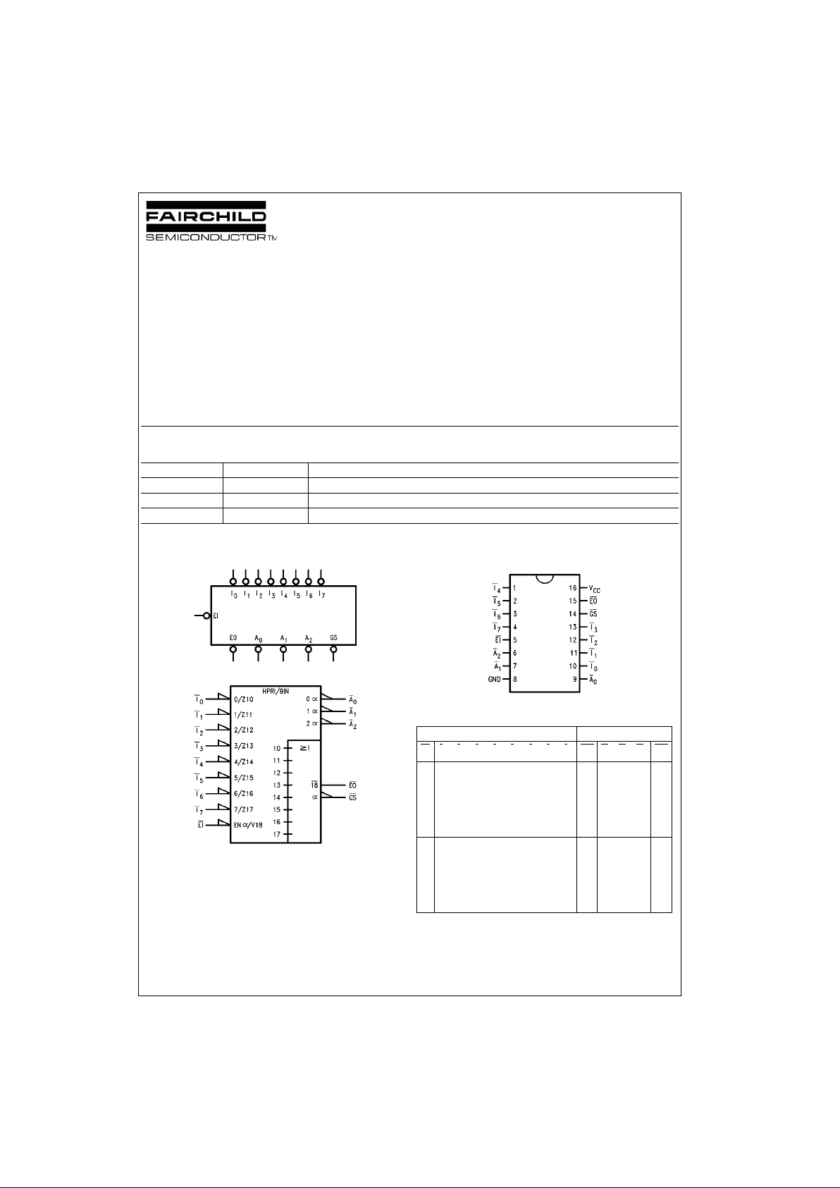
Logic Symbols
IEEE/IEC
Connection Diagram
Truth Table
H = HIGH Voltage Level
L = LOW Voltage Level
X = Immaterial
Order Number Package Number Package Description
74F148SC M16A 16-Lead Small Outline Integrated Circuit (SOIC), JEDEC MS-012, 0.150 Narrow
74F148SJ M16D 16-Lead Small Outline Package (SOP), EIAJ TYPE II, 5.3mm Wide
74F148PC N16E 16-Lead Plastic Dual-In-Line Package (PDIP), JEDEC MS-001, 0.300 Wide
Inputs Outputs
EI
I0I1I2I3I4I5I6I7GS A0A1A2EO
HXXXXXXXXHHHHH
LHHHHHHHHH HHH L
LXXXXXXXL LLLLH
LXXXXXXLH L HLL H
LXXXXXLHH L LHLH
LXXXXLHHHL HHLH
LXXXLHHHHLLLHH
LXXLHHHHH LHLHH
LXLHHHHHH L LHH H
LLHHHHHHH LHHH H
Page 2
www.fairchildsemi.com 2
74F148
Unit Loading/Fan Out
Functional Description
The F148 8-input priority e ncoder accept s data from ei ght
active LOW inputs (I
0–I7
) and provides a binary repr esen-
tation on the three active LOW outputs. A priority is
assigned to each input so that when two or more inputs are
simultaneously active , the input with the hig hest priority is
represented on the output, with input line 7 having the highest priority. A HIGH on the Enable Input (EI
) will force all
outputs to the inactive ( HIGH) state an d allow new data to
settle without pr oducing erroneous information at the out-
puts.A Group Signal outp ut (GS
) and Enable Output ( EO)
are provided along with the three priority data outputs (A
2
,
A
1
, A0). GS is active LOW when any input is LOW: this
indicates when any input is active. EO
is active LOW when
all inputs are HIGH. Usi ng the Enable Output along with
the Enable Input allows casc ading for priority en coding on
any number of inp ut signals. Both EO
and GS are in the
inactive HIGH state when the Enable Input is HIGH.
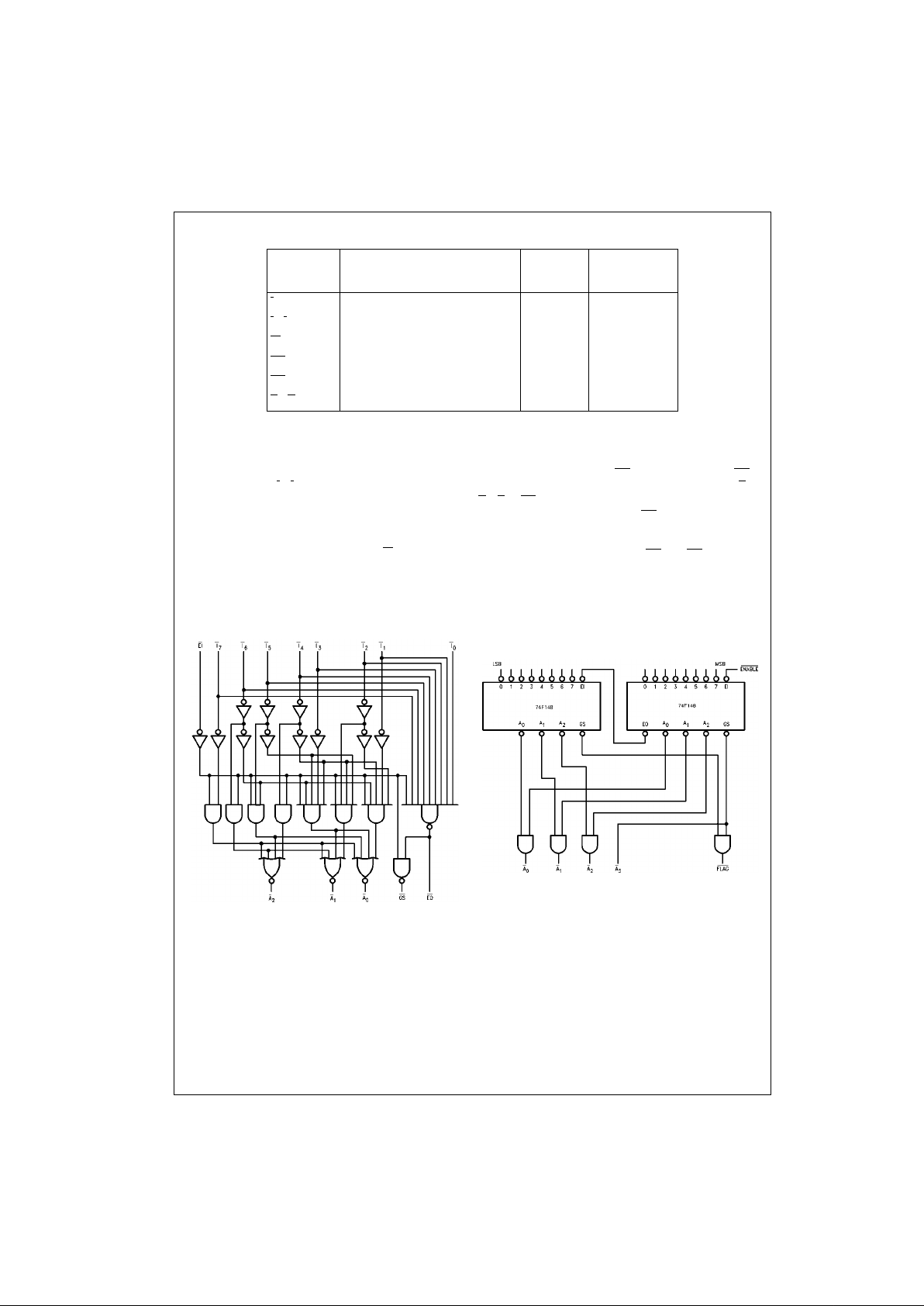
Logic Diagram
Please note that this diagram is provided only for the understanding of logic
operations and should not be used to est im at e propagation delays.
Application
16-Input Priority Encoder
Pin Names Description
U.L.
Input I
IH/IIL
HIGH/LOW
Output I
OH/IOL
I
0
Priority Input (Active LOW) 1.0/1.0 20 µA/−0.6 mA
I
1–I7
Priority Inputs (Active LOW) 1.0/2.0 20 µA/−1.2 mA
EI
Enable Input (Active LOW) 1.0/1.0 20 µA/−0.6 mA
EO
Enable Output (Active LOW) 50/33.3 −1 mA/20 mA
GS
Group Signal Output (Active LOW) 50/33.3 −1 mA/20 mA
A
0–A2
Address Outputs (Active LOW) 50/33.3 −1 mA/20 mA
Page 3

3 www.fairchildsemi.com
74F148
Absolute Maximum Ratings(Note 1) Recommended Operating
Conditions
Note 1: Absolute maximum ratings are values beyon d which the device
may be damaged or have its useful life impaired . Functional operation
under these condit ions is not implied.
Note 2: Either voltage limit or curren t limit is sufficient to protect in puts.
DC Electrical Characteristics
Storage Temperature −65°C to +150°C
Ambient Temperature under Bias −55°C to +125°C
Junction Temperature under Bias −55°C to +150°C
V
CC
Pin Potential to Ground Pin −0.5V to +7.0V
Input Voltage (Note 2) −0.5V to +7.0V
Input Current (Note 2) −30 mA to +5.0 mA
Voltage Applied to Output
in HIGH State (with V
CC
= 0V)
Standard Output −0.5V to V
CC
3-STATE Output −0.5V to +5.5V
Current Applied to Output
in LOW State (Max) twice the r ated I
OL
(mA)
Free Air Ambi ent Temperature 0°C to +70°C
Supply Voltage +4.5V to +5.5V
Symbol Parameter Min Typ Max Units
V
CC
Conditions
V
IH
Input HIGH Voltage 2.0 V Recognized as a HIGH Signal
V
IL
Input LOW Voltage 0.8 V Recognized as a LOW Signal
V
CD
Input Clamp Diode Voltage −1.2 V Min IIN = −18 mA
V
OH
Output HIGH 10% V
CC
2.5
VMin
IOH = −1 mA
Voltage 5% V
CC
2.7 IOH = −1 mA
V
OL
Output LOW 10% V
CC
0.5 V Min IOL = 20 mA
Voltage
I
IH
Input HIGH
5.0 µAMaxVIN = 2.7V
Current
I
BVI
Input HIGH Current
7.0 µAMaxVIN = 7.0V
Breakdown Test
I
CEX
Output High
50 µAMaxV
OUT
= V
CC
Leakage Current
V
ID
Input Leakage
4.75 V 0.0
IID = 1.9 µA
Test All Other Pins Grounded
I
OD
Output Leakage
3.75 µA0.0
V
IOD
= 150 mV
Circuit Current All Other Pins Grounded
I
IL
Input LOW −0.6 mA
Max
VIN = 0.5V (I0, EI)
Current −1.2 mA
VIN = 0.5V (I1–I7)
I
OS
Output Short-Circuit Current −60 −150 mA Max V
OUT
= 0V
I
CCH
Power Supply Current 35 mA Max VO = HIGH
I
CCL
Power Supply Current 35 mA Max VO = LOW
Page 4

www.fairchildsemi.com 4
74F148
AC Electrical Characteristics
Symbol Parameter
TA = +25°CT
A
= 0°C to +70°C
Units
VCC = +5.0V VCC = +5.0V
CL = 50 pF CL = 50 pF
Min Typ Max Min Max
t
PLH
Propagation Delay 3.0 7.0 9.0 3.0 10.0
ns
t
PHL
In to A
n
3.0 8.0 10.5 3.0 12.0
t
PLH
Propagation Delay 2.5 5.0 6.5 2.5 7.5
ns
t
PHL
In to EO
2.5 5.5 7.5 2.5 8.5
t
PLH
Propagation Delay 2.5 7.0 9.0 2.5 10.0
ns
t
PHL
In to GS
2.5 6.0 8.0 2.5 9.0
t
PLH
Propagation Delay 2.5 6.5 8.5 2.5 9.5
ns
t
PHL
EI to A
n
2.5 6.0 8.0 2.5 9.0
t
PLH
Propagation Delay 2.5 5.0 7.0 2.5 8.0
ns
t
PHL
EI to GS
2.5 6.0 7.5 2.5 8.5
t
PLH
Propagation Delay 2.5 5.5 7.0 2.5 8.0
ns
t
PHL
EI to EO
3.0 8.0 10.5 3.0 12.0
Page 5

5 www.fairchildsemi.com
74F148
Physical Dimensions inches (millimeters) unless otherwise noted
16-Lead Small Outline Integrated Circuit (SOIC), JEDEC MS-012, 0.150 Narrow
Package Number M16A
16-Lead Small Outline Package (SOP), EIAJ TYPE II, 5.3mm Wide
Package Number M16D
Page 6

www.fairchildsemi.com 6
74F148 8-Line to 3-Line Priority Encoder
Physical Dimensions inches (millimeters) unless otherwise noted (Continued)
16-Lead Plastic Dual-In-Line Package (PDIP), JEDEC MS-001, 0.300 Wide
Package Number N16E
Fairchild does not assume any responsibility for use of any circuitry described, no circuit pate nt licenses are implied and
Fairchild reserves the right at any time without notice to change said circuitry and specifications.
LIFE SUPPORT POLICY
FAIRCHILD’S PRODUCTS ARE NOT AUTHORIZED FOR USE AS CRITICAL COMPONENTS IN LIFE SUPPORT
DEVICES OR SYSTEMS WITHOUT THE EXPRESS WRITTEN APPROVAL OF THE PRESIDENT OF FAIRCHILD
SEMICONDUCTOR CORPORATION. As used herein:
1. Life support devices or systems are devices or systems
which, (a) are intended for surgical implant into the
body, or (b) support or sustain life, and (c) whose failure
to perform when properly used in accordance with
instructions for use provided in the labeling, can be reasonably expected to result in a significant inju ry to the
user.
2. A critical component in any componen t of a life su pport
device or system whose failu re to perform can be reasonably expected to ca use the fa i lure of the life su pp ort
device or system, or to affect its safety or effectiveness.
www.fairchildsemi.com
 Loading...