

Fairchild Semiconductor 74ACT323PC, 74ACT323CW Datasheet
June 1988
Revised October 1998
74ACT323 8-Bit Universal Shift/Storage Register with Synchronous Reset and Common I/O Pins
© 1999 Fairchild Semiconductor Corporation DS009787.prf www.fairchildsemi.com
74ACT323
8-Bit Universal Shift/Storage Register with
Synchronous Reset and Common I/O Pins
General Description
The ACT323 is an 8-bit universal shift/storage r egist er with
3-STATE outputs. Parallel load inputs and flip-flop outputs
are multiplexed to minimize pin count. Separate serial
inputs and outputs are provided for Q
0
and Q7 to allow
easy cascading. Four operation modes are possible: hold
(store), shift left, shift right and parallel load.
Features
■ ICC and IOZ reduced by 50%
■ Common parallel I/O for reduced pin count
■ Additional serial inputs and outputs for expansion
■ Four operating modes: shift left, shift right, load and
store
■ 3-ST ATE outputs for bus-oriented applications
■ Outputs source/sink 24 mA
■ TTL-compatible inputs
Ordering Code:
Device also available in Tape and Reel. Specify by appendin g s uf f ix let te r “X” to the ordering cod e.
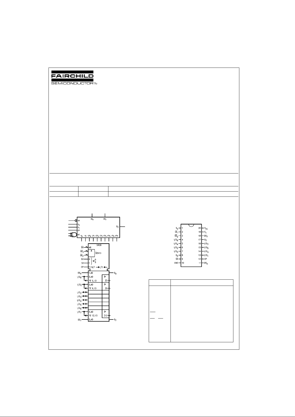
Logic Symbols Connection Diagram
Pin Assignment
for DIP
Pin Descriptions
FACT is a tra demark of Fairchild Semico nductor Corporat ion.
Order Number Package Number Package Description
74ACT323PC N20A 20-Lead Plastic Dual-In-Line Package (PDIP), JEDEC MS-001, 0.300” Wide
Pin Name Description
CP Clock Pulse Input
DS
0
Serial Data Input for Right Shift
DS
7
Serial Data Input for Left Shift
S
0
, S
1
Mode Select Inputs
SR
Synchronous Reset Input
OE
1
, OE23-STATE Output Enable Inputs
I/O
0
–I/O7Multiplexed Paralle l Data Inputs or
3-STATE Parallel Data Outputs
Q
0
, Q
7
Serial Outputs
www.fairchildsemi.com 2
74ACT323
Functional Description
The ACT323 contains eight edge-triggered D-type flip-flops
and the interstage logic necessary to perform synchronous
reset, shift left, shift right, parallel load and hold operations.
The type of operation is determined by S
0
and S1 as shown
in the Mode Select Table. All flip-flop outputs are brought
out through 3-STATE buffers to separate I/O pins that also
serve as data inp uts in the paralle l load mode. Q
0
and Q
7
are also brought out on othe r pins for expansion in serial
shifting of longer words.
A LOW signal on SR
overrides the Select inputs and allows
the flip-flops to be reset by the next rising edge of CP. All
other state changes are al so initi ated by the LOW-to-HIGH
CP transition. Inputs can change when the clock is in either
state provided only that th e recommend ed setup and h old
times, relative to the rising edge of CP, are observed.
A HIGH signal on either O E
1
or OE2 disables the 3-STATE
buffers and puts the I/O pins in the high impedance state.
In this condition the shift , load, hold and reset operati ons
can still occur. The 3-STATE buffers are also disabled by
HIGH signals on both S
0
and S1 in preparation for a paral-
lel load operation.
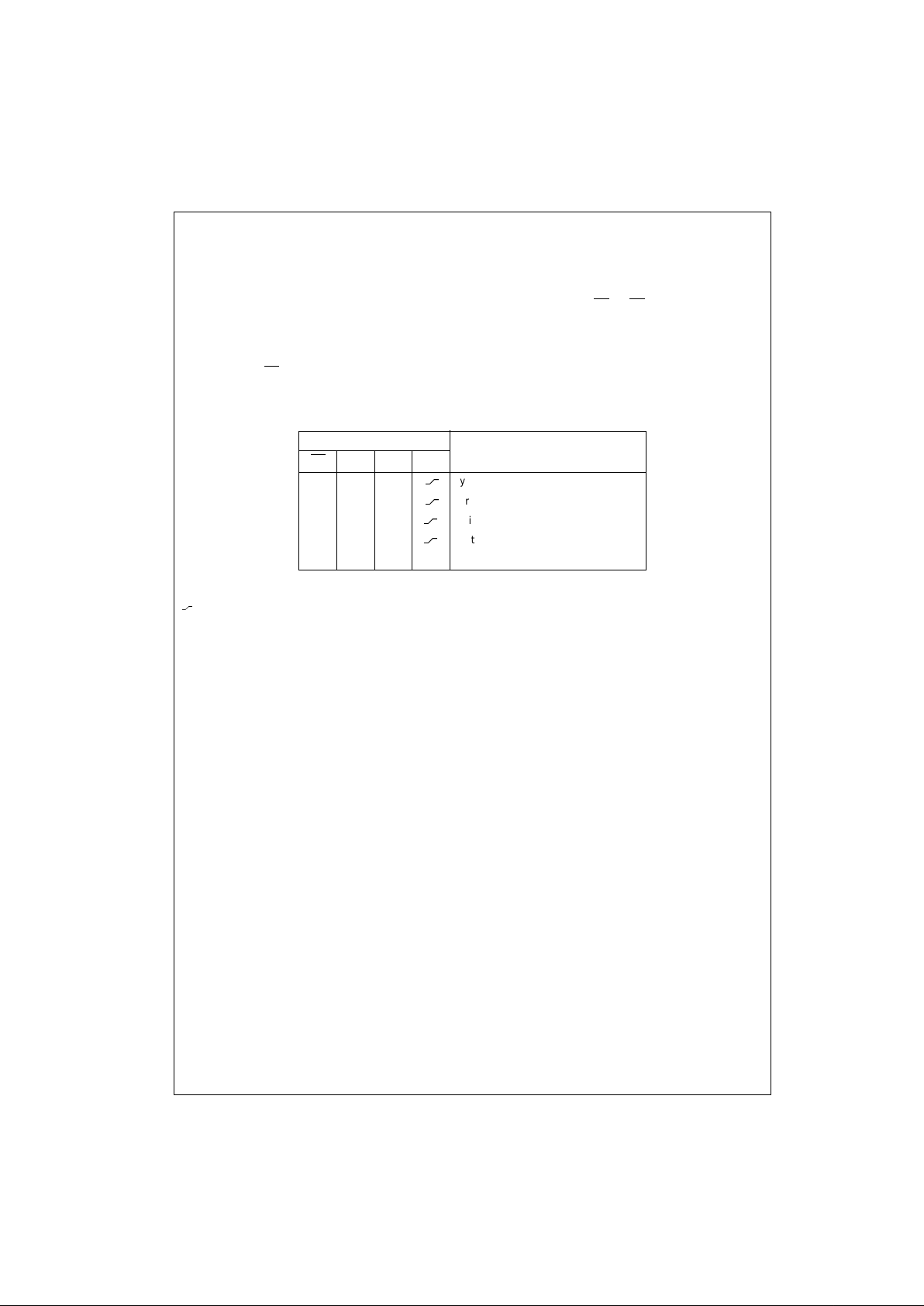
Mode Select Table
H = HIGH Voltage Level
L = LOW V oltage Lev el
X = Immaterial
= LOW-to-HIGH Clock Transition
Inputs Response
SR
S1S0CP
LXX
Synchronous Reset; Q0–Q7 = LOW
HHH
Parallel Load; I/On→Q
n
HLH Shift Right; DS0→Q0, Q0→Q1, etc.
HH L
Shift Left; DS7→Q7, Q7→Q6, etc.
H L L X Hold
 Loading...