Fairchild Semiconductor 74ACQ646SPC, 74ACQ646SCX, 74ACQ646SC, 74ACQ646CW Datasheet

© 2000 Fairchild Semiconductor Corporation DS010635 www.fairchildsemi.com
January 1990
Revised September 2000
74ACQ646 • 74ACTQ646 Quiet Series
Octal Tra nsceiver/Register with 3-STATE Outputs
74ACQ646 • 74ACTQ646
Quiet Series
Octal Transceiver/Register
with 3-STATE Outputs
General Description
The ACQ/ACTQ646 consis t of registered bus transceiver
circuits, with outputs, D-type flip-flops, and co ntrol circu itry
providing multiplexed transmission of data directly from the
input bus or fr om th e in t er na l sto r ag e r eg is t er s. Da t a on the
A or B bus will be loaded into the respective registers on
the LOW-to-HIGH transition of the appropriate clock pin
(CPAB or CPBA). The four fundamental handling functions
available are illustrated in Figure 1, Figure 2, Figure 3 and
Figure 4.
The ACQ/ACTQ utilizes Fairchild Quiet Series
technol-
ogy to guarantee quiet output switching and improved
dynamic threshold perf ormance. FACT Quiet Series
fea-
tures GTO
output control and undershoot corrector in
addition to a split ground bus for superior performance.
Features
■ Guaranteed simultaneous switching noise level and
dynamic threshold performan ce
■ Guarante ed pin-to-pin skew AC performance
■ Independent registers for A and B busses
■ Multiplexed real-time and stored data transfers
■ 300 mil slim dual-in-line package
■ Outputs source/sink 24 mA
■ Faster prop delays than the standard AC/ACT646
Ordering Code:
Device also available in Tape and Reel. Specify by appending s uffix let te r “X” to the ordering code.
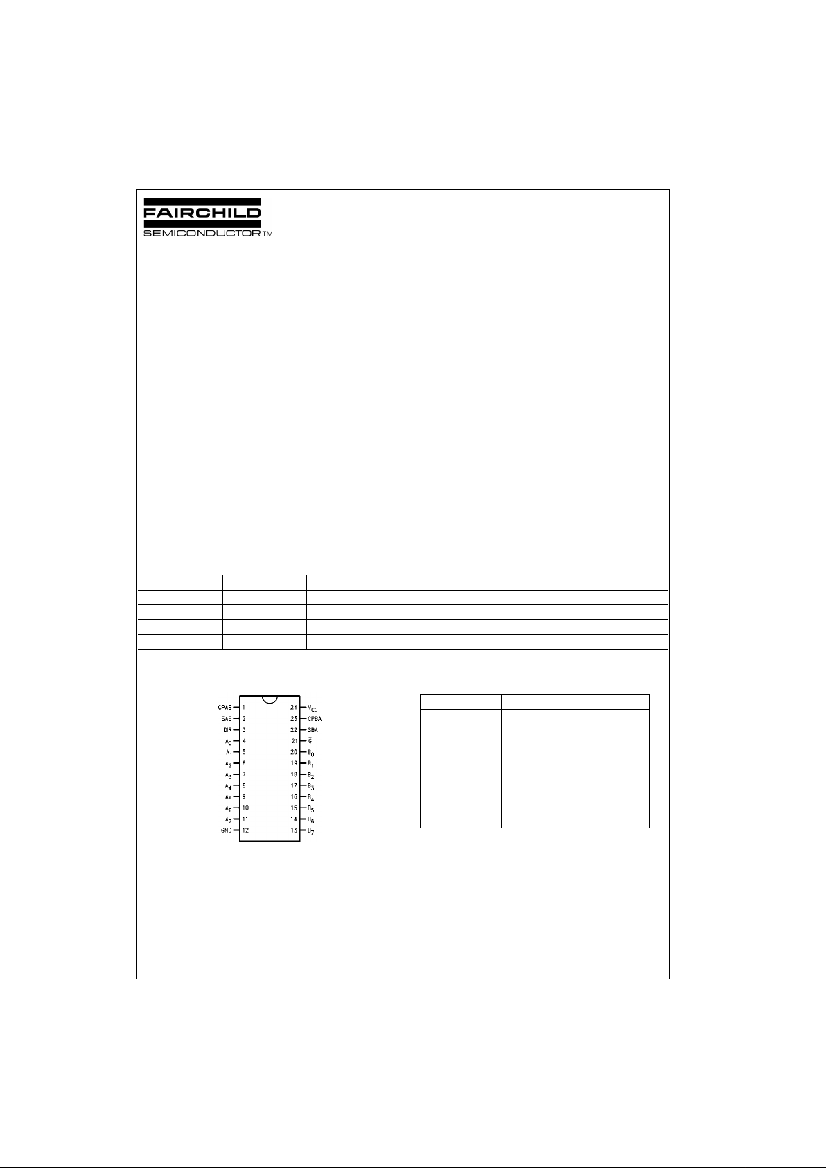
Connection Diagram Pin Descriptions
FACT, Qui et Series , FACT Quiet Series and GTO are trademarks of Fairchild Semiconductor Corporation
Order Number Package Number Package Description
74ACQ646SC M24B 24-Lead Small Outline Integrated Circuit (SOIC), JEDEC MS-013, 0.300 Wide
74ACQ464ASPC N24C 24-Lead Plastic Dual-In-Line Package (PDIP), JEDEC MS-001, 0.300 Wide
74ACTQ646SC M24B 24-Lead Small Outline Integrated Circuit (SOIC), JEDEC MS-013, 0.300 Wide
74ACTQ464ASPC N24C 24-Lead Plastic Dual-In-Line Package (PDIP), JEDEC MS-001 , 0.300 Wide
Pin Names Descriptions
A
0–A7
Data Register A Inputs
Data Register A Outputs
B
0–B7
Data Register B Inputs
Data Register B Outputs
CPAB, CPBA Clock Pulse Inputs
SAB, SBA Transmit/Receive Inputs
G
Output Enable Input
DIR Direction Control Input

www.fairchildsemi.com 2
74ACQ646 • 74ACTQ646
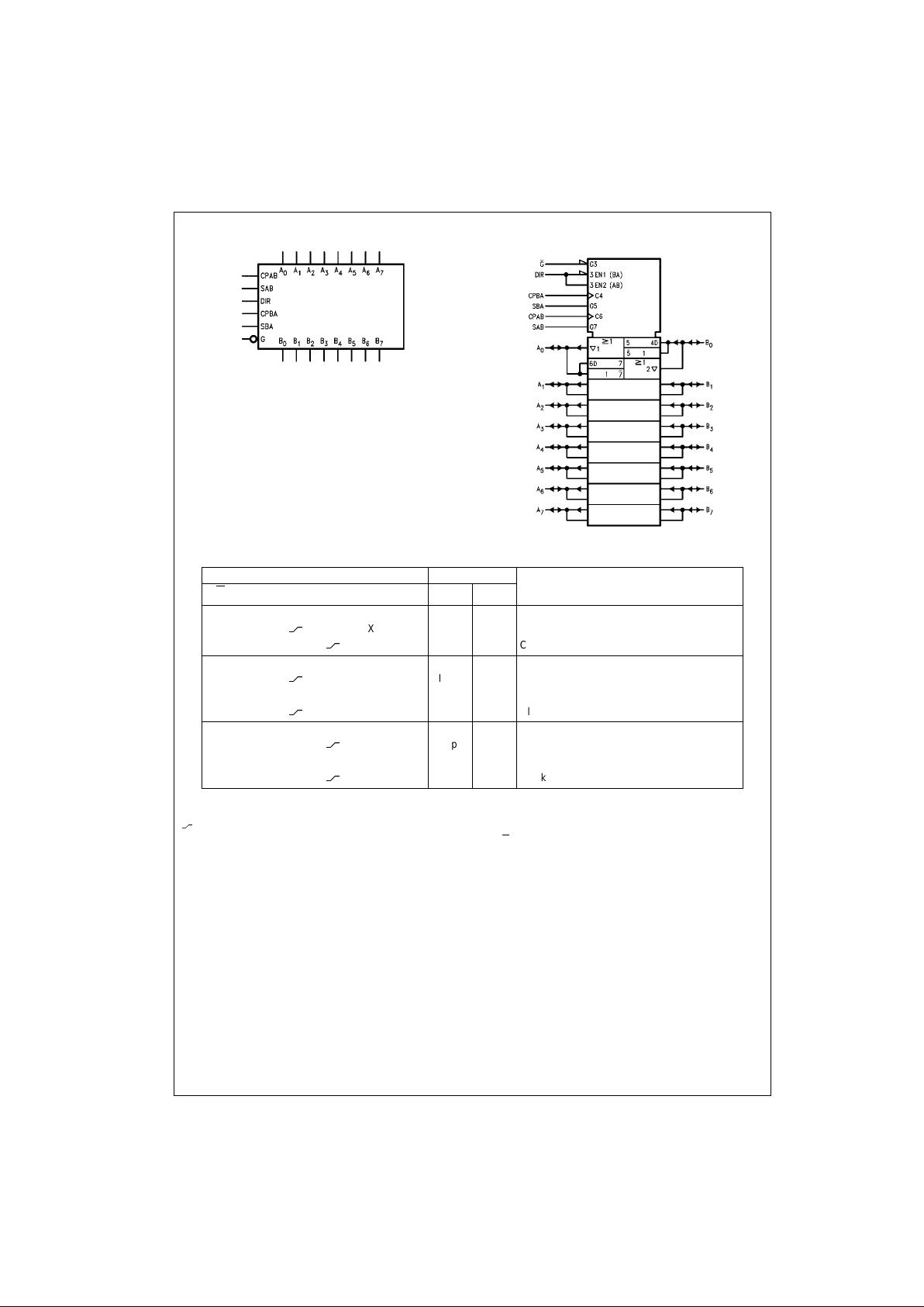
Logic Symbols
IEEE/IEC
Function Table
H = HIGH Voltage Level
L = LOW Voltage Level
X = Immaterial
= LOW-to-HIGH Transition
Note 1: The data output functions may be enabled or disabled by various signals at the G
and DIR input s . D ata input functions are al w ay s enabled; i.e. , data
at the bus pins will be s to red on every LOW-to-HIG H tra ns it ion of the appropriate clo c k inputs.
Inputs Data I/O (Note 1)
Function
G
DIR CPAB CPBA SAB SBA A0–A7B0–B
7
H X H or L H or L X X Isolation
HX
X X X Input Input Clock An Data into A Register
HXX
X X Clock Bn Data into B Register
LHXXLX A
n
to Bn—Real Time (Transparent Mode)
LH
X L X Input Output Clock An Data into A Register
L H H or L X H X A Register to B
n
(Stored Mode)
LH
X H X Clock An Data into A Register and Output to B
n
LLXXXL Bn to An—Real Time (Transparent Mode)
LLX
X L Output Input Clock Bn Data into B Register
L L X H or L X H B Register to A
n
(Stored Mode)
LLX
X H Clock Bn Data into B Register and Output to A
n

3 www.fairchildsemi.com
74ACQ646 • 74ACTQ646
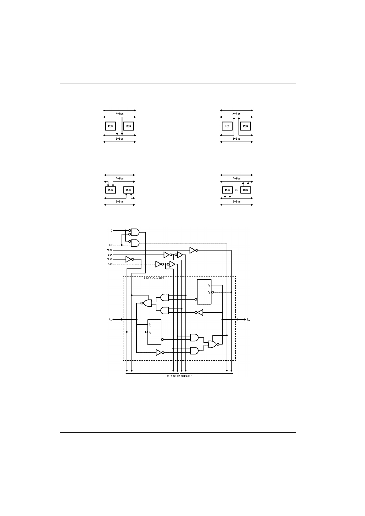
Real Time Transfer
A-Bus to B-Bus
FIGURE 1.
Real Time Transfer
B-Bus to A-Bus
FIGURE 2.
Storage from
Bus to Regi ster
FIGURE 3.
Transfer from
Register to Bus
FIGURE 4.
Logic Diagram
Please note that this diagram is provided only for the understanding of logic operations and should not be used to estimate propagation delays.
 Loading...