Fairchild (Now ON) LL4148, LL4148 Schematic [ru]

April 2013
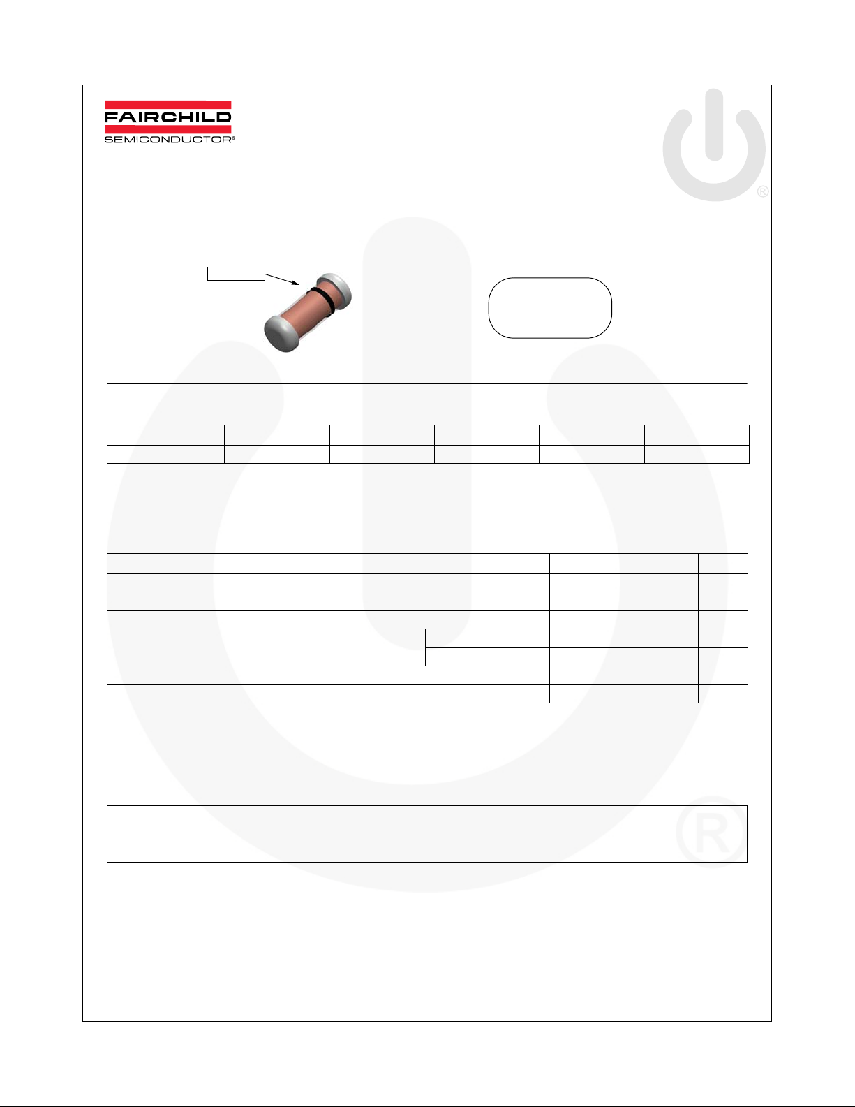
COLOR BAND MARKING
1ST BAND
Black
The 1st Band indicates the cathode band
SOD80
Cathode Band
LL4148
Small Signal Diode
Package Marking and Ordering Information
Device Marking Device Package Reel Size Tape Width Quantity
Color Band Marking LL4148 SOD80 7” 8 mm 2,500
LL4148 — Small Signal Diode
Absolute Maximum Ratings
Stresses exceeding the absolute maximum ratings may damage the device. The device may not function or be operable above the recommended operating co nd iti ons an d s tres si ng the parts to these levels is not reco mme nde d. In addition, extended exposure to stresses above the recommended operating conditions may affect device reliability. The
absolute maximum ratings are stress ratings only. Values are at T
(1)
= 25°C unless otherwise noted.
A
Symbol Parameter Value Units
V
RRM
I
F(AV)
I
I
FSM
T
STG
T
Note:
1. These ratings are limiting values above which the serviceability of the diode may be impaired.
These ratings are based on a maximum junction temperature of 200 °C.
These are steady state limits. The factory should be consulted on applications involving pulsed or low duty cycle
operations.
Thermal Characteristics
Maximum Repetitive Reverse Voltage 100 V
Average Rectified Forward Current 200 mA
Recurrent Peak Forward Current 500 mA
f
Non-repetitive Peak Forward Surge Current
Pulse Width = 1.0 s 1.0 A
Pulse Width = 1.0 μs2.0 A
Storage Temperature Range -65 to +200 °C
Operating Junction Temperature Range -55 to +175 °C
J
(2)
Symbol Parameter Value Units
P
R
θJA
Note:
2. Jedec Standard 51-3 method (PCB Board size 76*114*0.6Tmm3)
Power Dissipation 500 mW
D
Thermal Resistance, Junction to Ambient 300 °C/W
© 2005 Fairchild Semiconductor Corporation www.fairchildsemi.com
LL4148 Rev. 1.2.0 1

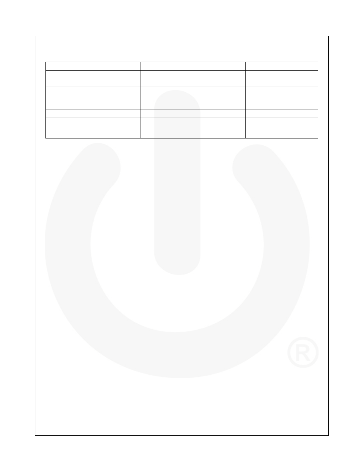
Electrical Characteristics
Values are at T
Symbol Parameter Conditions Min. Max. Units
V
R
V
F
I
R
C
T
t
rr
= 25°C unless otherwise noted.
A
I
= 100 μA100 V
Breakdown Voltage
R
I
= 5.0 μA75 V
R
Forward Voltage IF = 10 mA 1.0 V
V
= 20 V 25 nA
Reverse Leakage
R
= 20 V, TA = 150°C50μA
V
R
Total Capacitance VR = 0, f = 1.0 MHz 4.0 pF
I
= 10 mA, VR = 6.0 V
Reverse Recovery Time
F
(60 mA),
= 1.0 mA, RL = 100 Ω
I
rr
4.0 ns
LL4148 — Small Signal Diode
© 2005 Fairchild Semiconductor Corporation www.fairchildsemi.com
Rev. 1.2.0 2

Typical Performance Characteristics
110
120
130
140
150
160
Ta=25 oC
1 2 3 5 10 20 30 50 100
Reverse Voltage, V
R
[V]
Reverse Current, IR [uA]
V
R
0
20
40
60
80
100
120
10 20 30 50 70 1 0 0
Ta= 25 oC
Reverse Current, I
R
[nA]
Reverse Voltage, VR [V]
Reverse Voltage, VR [V]
I
R
250
300
350
400
450
500
550
1 2 3 5 10 20 30 50 1 0 0
Ta= 25 oC
Forward Voltage, V
R
[mV]
Forward Cu rre n t, IF [uA]
V
F
450
500
550
600
650
700
750
0.1 0.2 0.3 0.5 1 2 3 5 10
Ta= 25 oC
Forward Voltage, V
F
[mV]
Forward Current, IF [mA]
V
F
0.6
0.8
1.0
1.2
1.4
1.6
10 20 30 50 100 200 300 500 800
Ta= 25 oC
Forward Voltage, V
F
[mV]
Forward Current, IF [mA]
[
V
F
0.01 0.1 1 10
300
400
500
600
700
800
900
3
0.3
0.03
Typical
Ta= -40 oC
Ta= 25 oC
Ta= +65 oC
Forward Voltage, V
F
[mV]
Forward Current, IF [mA]
V
F
LL4148 — Small Signal Diode
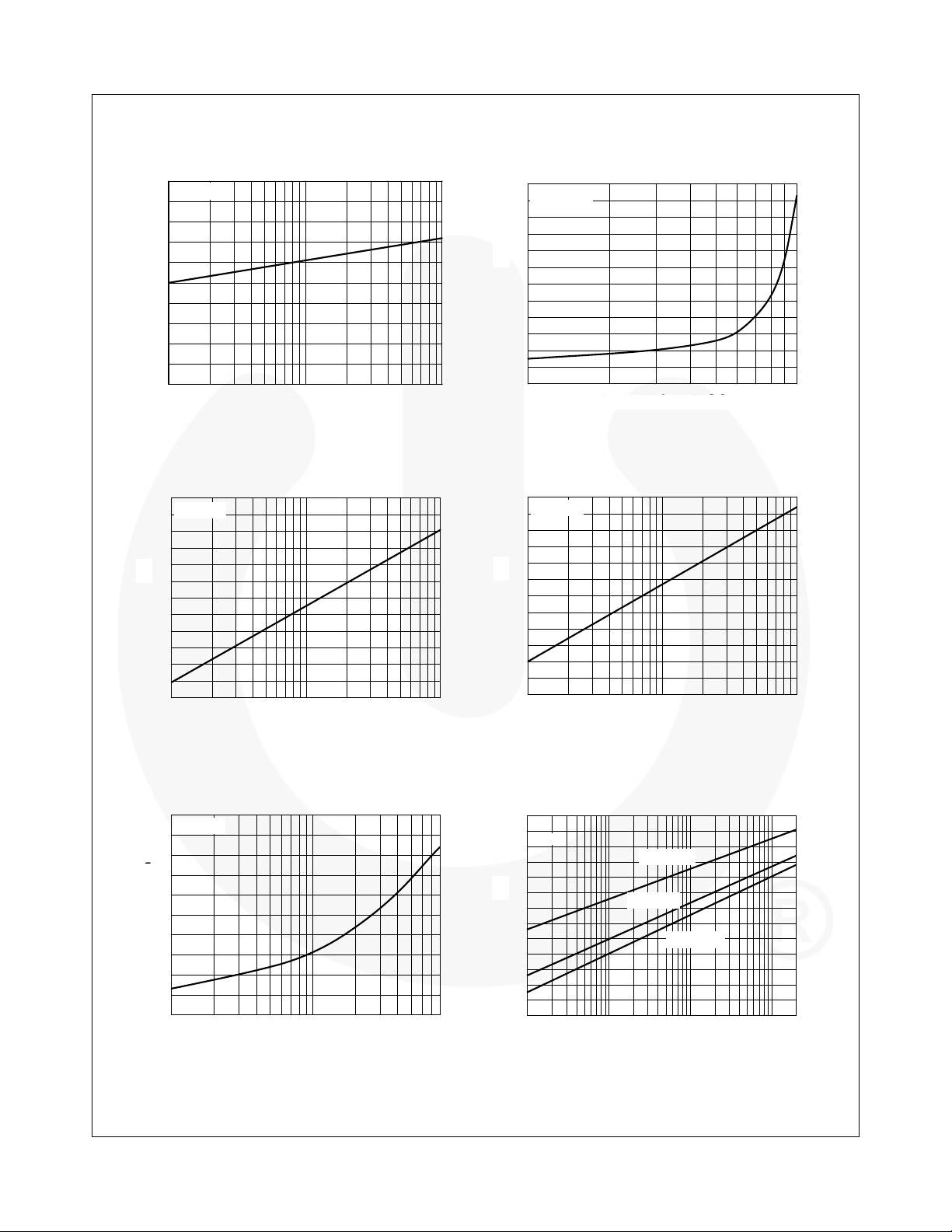
Figure 1. Reverse Voltage vs Reverse Current
BV - 1.0 to 100 μA
Figure 3. Forward Voltage vs Forward Current
V
- 1 to 100 μA
F
Figure 2. Reverse Voltage vs Reverse Current
I
- 10 to 100 V
R
Figure 4. Forward Voltage vs Forward Current
- 0.1 to 10 mA
V
F
© 2005 Fairchild Semiconductor Corporation www.fairchildsemi.com
Rev. 1.2.0 3
Figure 5. Forward Voltage vs Forward Current
- 10 to 800 mA
V
F
Figure 6. Forward Voltage vs Ambient Temperature
VF - 0.01 - 20 mA (-40 to +65 Deg C)
 Loading...