

Fairchild (Now ON) FDMC8296 Schematic [ru]
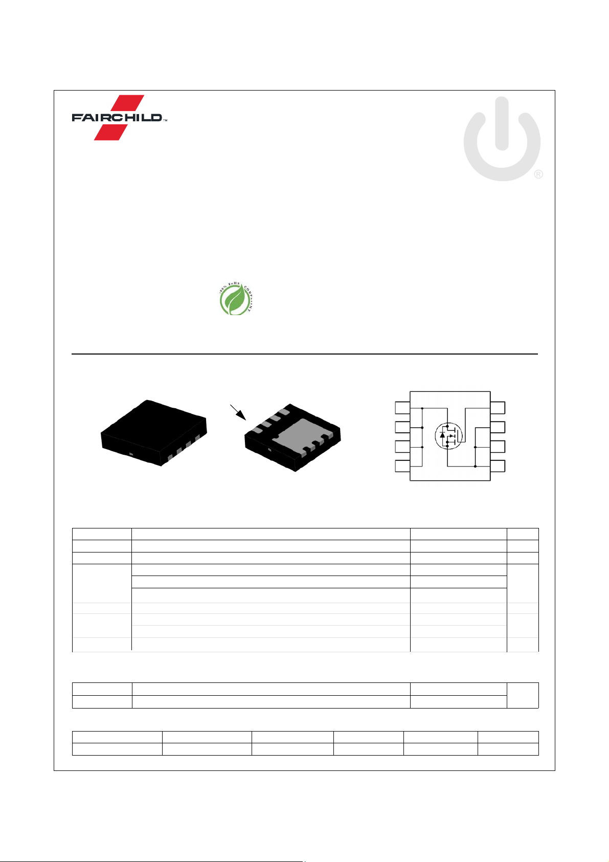
FDMC8296
N-Channel Power Trench®MOSFET
30V, 18A, 8.0m:
Features
Max r
Max r
High performance trench technology for extremely low r
Termination is Lead-free and RoHS Compliant
= 8.0m: at VGS = 10V, ID = 12A
DS(on)
= 13.0m: at VGS = 4.5V, ID = 10A
DS(on)
DS(on)
June 2014
General Description
This N-Channel MOSFET is produced using Fairchild
Semiconductor‘s advanced Power Trench
been especially tailored to minimize the on-state resistance. This
device is well
applications common in Notebook Computers and Portable
Battery Packs.
suited for Power Management and load switching
Application
DC - DC Buck Converter
Notebook battery power management
Load switch in N
otebook
®
process that has
FDMC8296 N-Channel Power Trench
®
MOSFET
Top
Bottom
G
S
S
S
D
D
D
D
5
D
D
6
D
7
8
D
MLP 3.3x3.3
MOSFET Maximum Ratings
Symbol Parameter Ratings Units
V
DS
V
GS
I
D
E
AS
P
D
T
J
STG
, T
Drain to Source Voltage 30 V
Gate to Source Voltage ±20 V
Drain Current -Continuous TC= 25°C 18
-Continuous TA= 25°C
-Pulsed
Single
P
ulse Avalanche Energy (Note 3)
Power Dissipation
Power D
Operating and Storage Junction Temperature Range
ssipation T
i
TA= 25°C unless otherwise noted
T
= 25°C
C
= 25°C
A
(Note 1a)
(Note 1a)
12
52
72
27
2.3
-55 to +150 °C
Thermal Characteristics
G
4
S
3
S
2
S
1
A
mJ
W
R
TJC
R
TJA
Thermal Resistance, Junction to Ca
Thermal Resistance, Junction to Ambient
Package Marking and Ordering Information
Device Marking Device Package Reel Size Tape Width Quantity
FDMC8296 FDMC8296 MLP 3.3X3.3 13 ’’
©2010 Fairchild Se
FDMC8296 Rev.C3
miconductor Corporation
se 4.6
(Note 1a) 53
12 mm 3000 units
1
°C/W
www.fairchildsemi.com
FDMC8296 N-Channel Power Trench
Electrical Characteristics
TJ = 25°C
unless otherwi
se noted
Symbol Parameter Test Conditions Min Typ Max Units
Off Characteristics
BV
'BV
'T
I
DSS
I
GSS
DSS
DSS
J
Drain to
Source Breakdown Voltage I
Breakdown
Voltage Temperature
Coefficient
Zero Gate V
Gate to Source Le
oltage Drain Current
akage Current V
= 250PA, VGS = 0
D
I
= 250PA, reference
D
= 24V, 1
V
DS
= 0V,
V
GS
±20V, V
=
GS
V 30 V
d to 25°C 17 mV/°C
=
T
125°C 250
J
= 0V
DS
±100 nA
On Characteristics
V
GS(th)
'V
GS(th)
'T
J
r
(on)
DS
g
FS
Dyn
amic Characteristics
C
iss
C
os
s
C
s
rs
R
g
Gate to Source T
Gate to Source Threshold V
hreshold Voltage V
oltage
Temperature Coefficient
S
tatic Drain to Source On Resistance
Forward T
Input C
Output Cap
ansconductance V
r
apacitance
acit
ance 513 685 pF
Reverse Transfer Capacitance 87 135 pF
Gate Resi
stance f = 1MHz 0.9 :
= VDS, ID = 250PA 1.
GS
= 250PA, referenced to
I
D
V
GS
GS
V
GS
DD
V
f = 1MHz
, I
= 10V
= 4.5V
= 10V
= 5V
= 15V, VGS = 0V,
DS
= 12A 6.5
D
= 10A 9.5
, I
D
= 12A, TJ = 125°
, I
D
, I
= 12A 44 S
D
25
°C -6 mV/°C
0 1.9 3.0 V
8.0
13.0
C 9.0 12.8
1
038 1385 pF
m:V
PA
®
MOSFET
Switching Char
t
n)
d(o
t
r
t
d(o
ff)
t
f
Q
g(T
OT)
Q
gs
Q
gd
acteristics
Turn-On Delay Time
Rise T
ime 310ns
T
urn-Off Delay Time 19 35 ns
all T
F
ime 210ns
T
otal Gate Charge
T
otal Gate Charge 3nC
Gate to Drain
Drain-Source Dio
V
SD
t
rr
Q
rr
NOTES:
1. R
is d
TJA
the user's board design.
Source to D
Reverse Recovery T
Reverse Recovery Charge 9
etermined with the device mounte d on a 1in
“Miller”
Charge 2.5 nC
de Characteristics
rain Diode Forward Voltage
ime
2
p
ad 2 oz copper pad on a 1.5 x 1.5 in. board of FR-4 material. R
a
. 53 °C/W when mounted on
a 1 i n
VDD = 15V, ID = 12A,
V
GS
VGS= 0V to 10V
V
GS
V
GS
V
GS
=
I
F
2
p
ad of 2 oz copper
= 10V, R
= 0V to 4
= 0V, IS=
= 0V,
= 6:
GEN
.5V 7.6 10.6 nC
V
DD
I
D
12A (Note 2) 0.82 1.3
=
I
1.9A (Note 2) 0.73 1.2
S
12A, di/dt = 100A/Ps
= 15V
= 12A
91
16
,
25 45 ns
i
s guaranteed by design while R
TJC
b.125 °C/W when mounted on
a minimum pad of 2 oz copper
8ns
23 nC
V
is de
nC
termined by
18
TCA
2. Pulse Test: Pulse Width < 300Ps, Duty cycle < 2.0%.
3. EAS of 72 mJ is based on starting T = 25 C, L = 1 mH, IAS = 12 A, VDD = 27 V, VGS = 10 V. 100% test at L = 3 mH, IAS= 5.7 A.
©2
010 Fairchild Semiconductor Corporation
FDMC8296 Rev.C
3
2
www.fa
irchildsemi.com
FDMC8296 N-Channel Power Trench
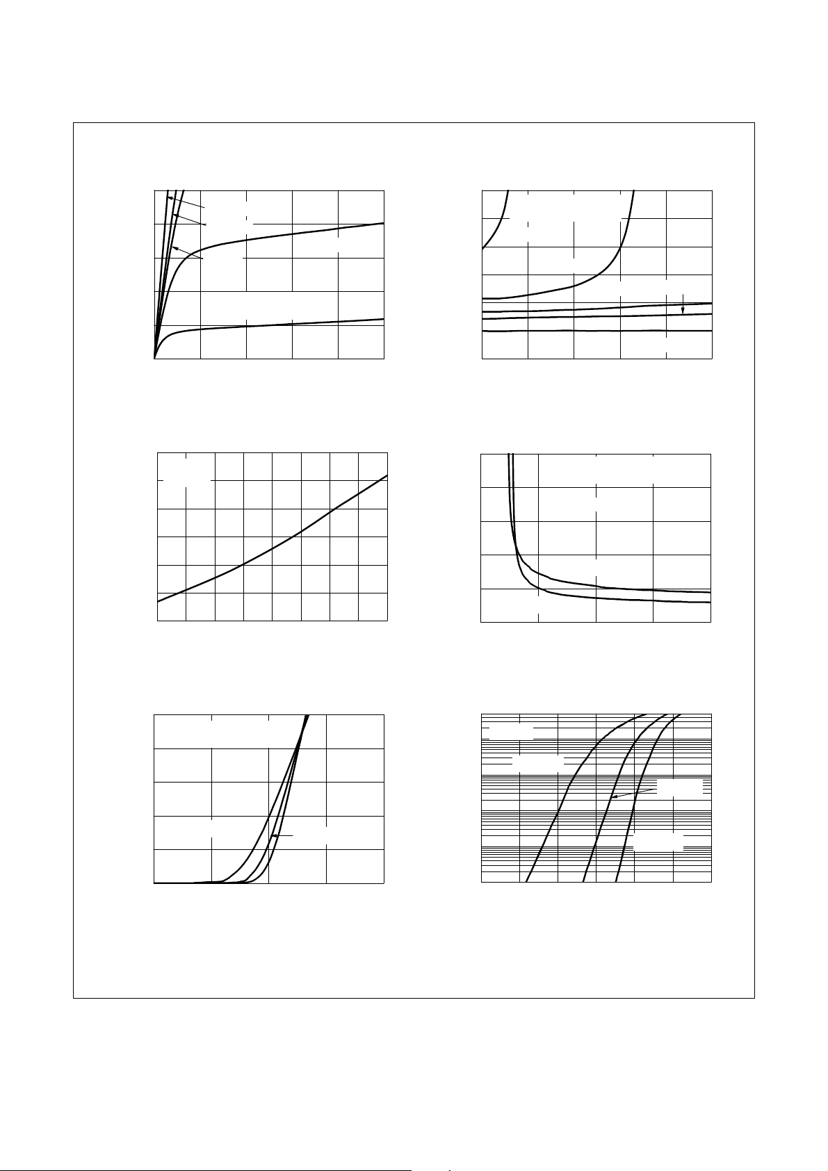
Typical Characteristics
50
VGS = 10V
40
30
20
IN CURRENT (A)
DRA
,
10
D
I
0
01
Figure 1.
1.8
ID = 12
V
1.6
1.4
LIZED
1.2
1.0
NORMA
0.8
DRAIN TO SOURCE ON-RESISTANCE
0.6
-5
0 -25 0 25 50 75 100 125 150
F i g u r e 3 . N o r m a l i z e d O n - R e s i s t a n c e
VGS = 4.5V
VGS = 4V
LSE DURATION = 80
PU
DUT
Y CYCLE = 0.5%MAX
2345
IN TO SOURCE VOLTAGE (V)
V
DRA
,
DS
On-Region Characteristics Figure 2.
A
V
= 10
GS
T
JU
,
NCTION TEMPERATURE
J
vs. Junction Temperature
TJ = 25°C unless otherw
VGS = 3.5V
P
s
VGS = 3V
o
(
C)
ise noted
6
PULSE DURATION = 80Ps
5
DUTY CYCLE = 0.5%MAX
VGS = 3V
4
ALIZED
NORM
3
2
VGS = 3.5V
V
V
= 4V
GS
GS
= 4.5V
1
V
=10
DRAIN TO SOURCE ON-RESISTANCE
0
0 1
020304050
N CURRENT(A)
,
I
DRAI
D
r m a l i z e d O n - R e s i s t a n c e
N o
GS
vs. Drain Current and Gate Voltage
50
)
:
m
40
(
TO
30
DRAIN
,
20
DS(on)
r
10
SOURCE ON-RESISTANCE
0
TJ= 25oC
246810
V
GAT
,
GS
n - R e si s t a n c e v s. G a t e t o
Figure 4.
O
SE DURATION = 80
PUL
DUTY CY
CLE = 0.5%MAX
A
ID= 12
TJ= 125oC
E TO SOURCE VOLTAGE (V)
P
s
Source Voltage
V
®
MOSFET
50
SE DURATION = 80
PUL
DUT
40
Y CYCLE = 0.5%MAX
VDS= 5V
30
20
DRAIN CURRENT (A)
,
10
D
I
0
12345
TJ= 150oC
VGS,
Figure 5. Transfer Characteristics
10 Fairchild Semiconductor Corporation
©20
FDMC8296 Rev.C3
s
P
TJ= 25oC
o
TJ= -5
C
5
GATE TO SOURCE VOLTAGE (V)
50
V
= 0V
GS
10
1
TJ= 150oC
TJ = 25oC
0.1
o
TJ = -5
C
EVERSE DRAIN CURRENT (A)
0.01
, R
S
I
0.001
0.0 0.2 0.4 0.6 0.8 1.0 1.2
Y DIODE FORWARD VOLTAGE (V)
VSD, BOD
Figu
re 6.
u r c e to D r a i n D i o de
S o
5
Forward Voltage vs. Source Current
3
www.fairchild
semi.com
 Loading...