Fairchild (Now ON) FAN7318M, FAN7318M Schematic [ru]
FAN7318
LCD Backlight Inverter Drive IC
FAN7318 — LCD Backlight Inverter Drive IC
June 2011
Features
High-Efficiency Single-Stage Power Conversion
Wide Input Voltage Range: 6V to 30V
Backlight Lamp Ballast and Soft Dimming
Minimal External Components Required
Precision Voltage Reference Trimmed to 2%
Half-Bridge Topology
Soft-Start
PWM Control at Fixed Frequency
Analog Dimming Function
Burst Dimming Function
Programmable Striking Frequency
Open-Lamp Protection
Open-Lamp Regulation
Short-Lamp Protection
CMP-High Protection
FB-High Protection
Thermal Shutdown
20-Pin SOIC
Applications
LCD TV
LCD Monitor
Description
The FAN7318 is a LCD backlight inverter drive IC that
controls P-N half-bridge topology.
The FAN7318 provides a low-cost solution and reduces
external components by integrating proprietary wave
rectifiers for open-lamp protection and regulation. The
operating voltage range of the FAN7318 is wide, so an
external regulator isn’t necessary to supply the voltage to
the IC.
The FAN7318 provides various protections, such as
open-lamp regulation, open-lamp protection, short-Lamp
protection, CMP-high protection, and FB-high protection,
to increase the system reliability. The FAN7318 provides
burst dimming and analog dimming.
The FAN7318 is available in a 20-SOIC package.
Ordering Information
Part Number
FAN7318M
FAN7318MX Tape & Reel
© 2009 Fairchild Semiconductor Corporation www.fairchildsemi.com
FAN7318 • 1.0.2
Operating
Temperature
-25 to +85°C 20-Lead, Small Outline Integrated Circuit (SOIC)
Package Packing Method
Rail
Block Diagram
FAN7318 — LCD Backlight Inverter Drive IC
OLR1
OLR2
OLR3
OLR4
CT
CMP
ADIM
OLP1
OLP2
OLP3
OLP4
Min. &
Max.
Detector
/Fu ll Wave
Recifier
Open Lamp Regulation
max. 2V
min. 0.5V
Soft start by first
BCT waveform
Negative
Analog
Dimm ing
OLP max .
Min. & Max.
Detector
/Full or Half
Rectifier
Min.
0.3V
Max.
1.34V
2V
1.34V
2.2V
Gm = 350, Max. current 70µA
On @ stri king
Source current
1.3uA @ CMP>2.5V
Error. Amp. source
current change
V
Error Amp.
ref
+
-
52µA burst
sink current on
3.5V
Disable @ striking
High_FB 8 pulses
count @ normal
Reset by BCT edge
detect
Wave
OLP min .
0.7V/0.5V
Striking/normal
Short Lamp Protection
-
+
Over- Voltage Protection
Protection
+
-
High_FB
+
-
+
-
-
0µA
3.2µA
Error. Amp. source
current change
Gm Amp.
+
Oscillator
-
+
0µA sink current @ striking
High CMP Protection
disable @ striking
+
3.5V
High FB Protection
disable @ striking
+
-
-
High_FB delay
-
+
High_CMP
Striking off
4 Output
Pulses
Counter
OLP
150µs
Delay
High_FB
52µA burst
sink current on
If ENA>2.5V, OLP & SLP disable.
If ENA<2.1V, OLP & SLP enable.
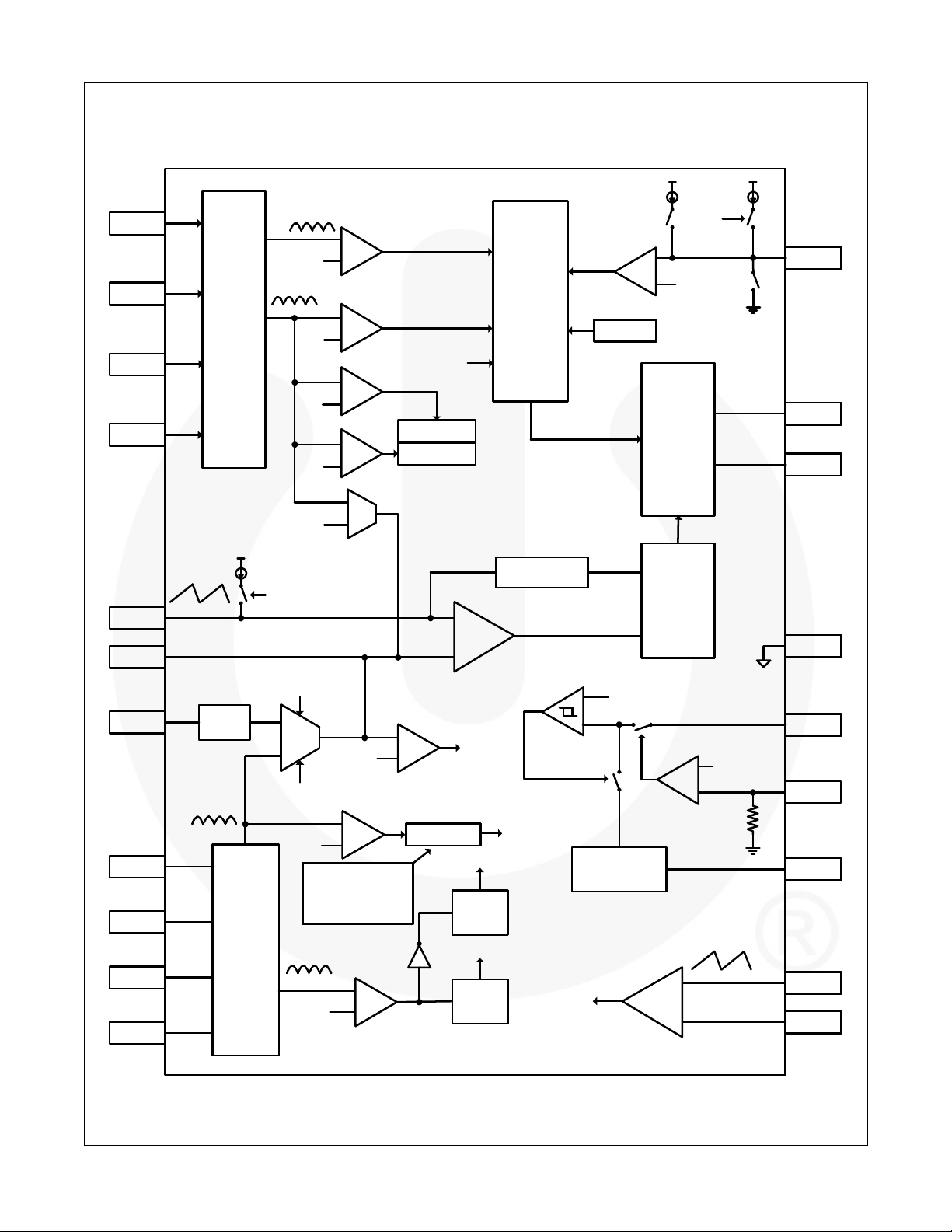
Figure 1. Internal Block Diagram
Hys. 0.45V
50µA
On @ OVP, SLP
TSD 150oC
-
+
UVLO 5.5V
Voltage Reference
& Internal Bias
Soft start by first
BCT waveform
On @
High_CMP, OLP
+
-
3V/1V
@ striking /normal
Output Driver
Control
Logic
-
+
5V, max. 3mA
max. 2V
min. 0.5V
-
disable @ striking
+
2µA
TIMER
OUTA
OUTB
GND
VIN
1.35V
ENA
200k
REF
BCT
BDIM
© 2009 Fairchild Semiconductor Corporation www.fairchildsemi.com
FAN7318 • 1.0.2 2
Pin Configuration
FAN7318 — LCD Backlight Inverter Drive IC
OLP1
20 19 18 17 16 15 14 13
OLR1
OLP2
OLR2
OLP3
OLR3
OLP4
OLR4
VIN
OUTA
12 11
1 2 3 4 5 6 7 8
TIMER
CMP
ADIM
CT
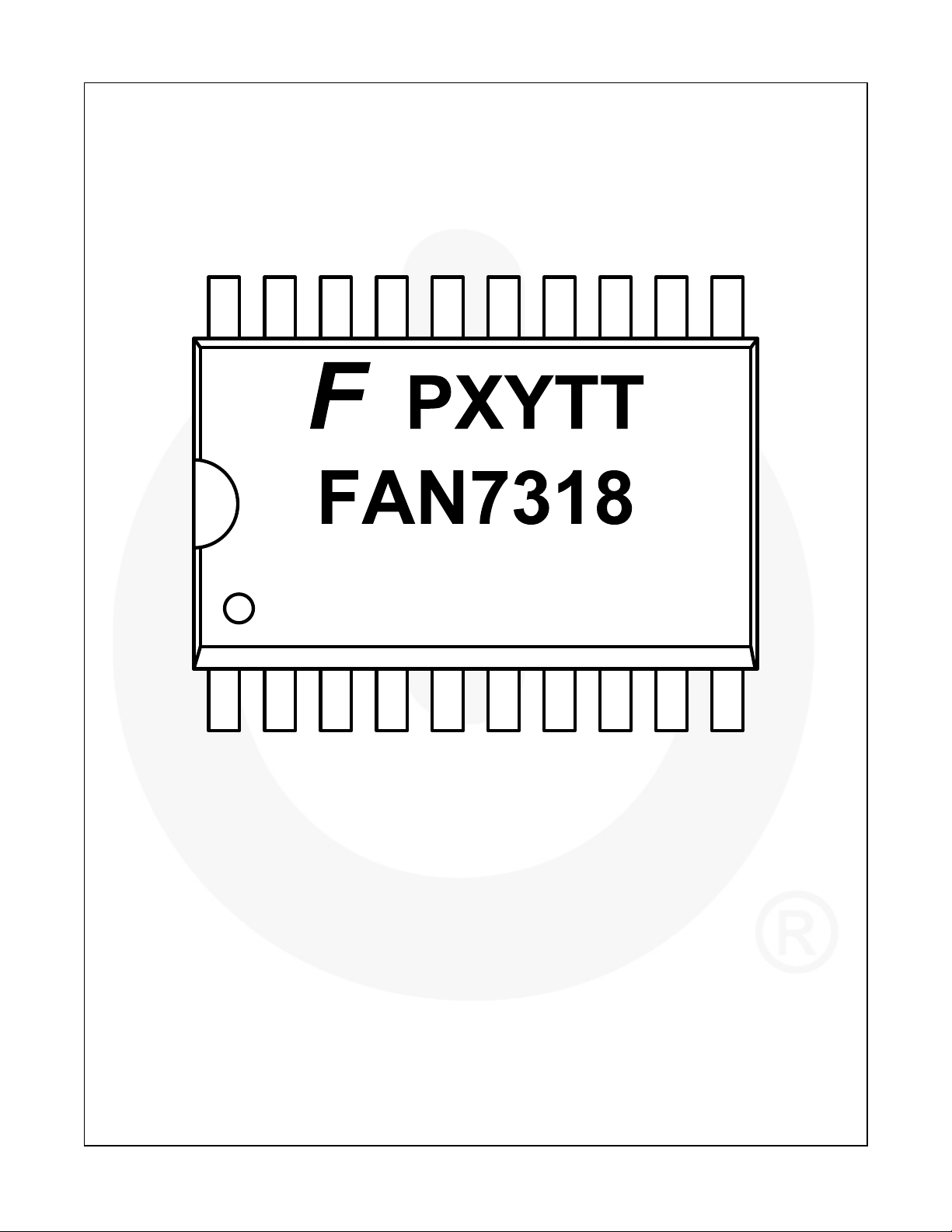
Figure 2. Package Diagram
REF
BCT
BDIM
ENA
9 10
GND
OUTB
© 2009 Fairchild Semiconductor Corporation www.fairchildsemi.com
FAN7318 • 1.0.2 3

Pin Definitions
Pin # Name Description
1 TIMER This pin is for protection delay time setting.
2 CMP
3 ADIM This pin is the input for negative analog dimming.
4 CT
5 REF
6 BCT
7 BDIM
8 ENA This pin is for turning on/off the IC.
9 GND This pin is the ground.
10 OUTB This pin is NMOS gate-drive output.
11 OUTA This pin is PMOS gate-drive output.
12 VIN This pin is the supply voltage of the IC.
13 OLR4 This pin is for open-lamp regulation. Its functions are the same as the OLR1 pin.
14 OLP4
15 OLR3 This pin is for open-lamp regulation. Its functions are the same as the OLR1 pin.
16 OLP3
17 OLR2 This pin is for open-lamp regulation. Its functions are the same as the OLR1 pin.
18 OLP2
19 OLR1
20 OLP1
Error amplifier output. Typically, a compensation capacitor is connected to this pin from the
ground.
This pin is for programming the switching frequency. Typically, a capacitor is connected to
this pin from ground and a resistor is connected to this pin from the REF pin.
This pin is 5V reference output. Typically, resistors are connected to this pin from the CT pin
and the BCT pin.
This pin is for programming the frequency of the burst dimming. Typically, a capacitor is
connected to this pin from ground and a resistor is connected to this pin from the REF pin.
This pin is the input for negative burst dimming. The voltage range of 0.5 to 2V at this pin
controls burst mode duty cycle from 0% to 100%.
This pin is for open-lamp protection and feedback control of lamp currents. Its functions are
the same as the OLP1 pin.
This pin is for open-lamp protection and feedback control of lamp currents. Its functions are
the same as the OLP1 pin.
This pin is for open-lamp protection and feedback control of lamp currents. Its functions are
the same as the OLP1 pin.
This pin is for open-lamp regulation and short-lamp protection. It has the same functions as
other OLR pins and is connected to the full-wave rectifier internally. When the maximum of
rectified OLR inputs is between 1.34V and 2V, the error amplifier output current is limited to
3.2µA; and when the maximum of rectified OLR inputs reaches 2V, the error amplifier output
current is 0A and its output voltage maintains constant. The maximum of rectified OLR
inputs is inputted to the negative of another error amplifier for feedback control of lamp
voltage. When the maximum of rectified OLR inputs is more than 2.2V, another error
amplifier for OLR is operating and lamp voltage is regulated. In normal mode, if the
maximum of rectified OLR inputs is higher than 1.35V or if the minimum of rectified OLR
inputs is lower than 0.3V for a predetermined time by the TIMER pin capacitor and a internal
current source 50µA, the IC shuts down to protect the system in over-voltage condition,
short-lamp condition, respectively.
This pin is for open-lamp protection and feedback control of lamp currents. It has the same
functions as other OLP pins and is connected to the half-wave rectifier and the full-wave
rectifier internally. In striking mode, if the minimum of rectified OLP inputs is less than 0.7V
for a predetermined time by the TIMER pin capacitor and an internal current source or, in
normal mode, if the minimum of rectified OLP inputs is less than 0.5V for another
predetermined time by the TIMER pin capacitor and another internal current source; the IC
shuts down to protect the system in open-lamp condition. The maximum of rectified OLP
inputs is inputted to the negative of the error amplifier for feedback control of lamp current.
FAN7318 — LCD Backlight Inverter Drive IC
© 2009 Fairchild Semiconductor Corporation www.fairchildsemi.com
FAN7318 • 1.0.2 4
Absolute Maximum Ratings
Stresses exceeding the absolute maximum ratings may damage the device. The device may not function or be
operable above the recommended operating conditions and stressing the parts to these levels is not recommended. In
addition, extended exposure to stresses above the recommended operating conditions may affect device reliability.
The absolute maximum ratings are stress ratings only.
Symbol Parameter Min. Max. Unit
VIN IC Supply Voltage 6 30 V
TA Operating Temperature Range -25 +85
TJ Operating Junction Temperature +150
T
Storage Temperature Range -65 +150
STG
θJA Thermal Resistance Junction-Air
PD Power Dissipation 1.4 W
Notes:
1. Thermal resistance test board; size: 76.2mm x 114.3mm x 1.6mm (1S0P); JEDEC standard: JESD51-2, JESD51-3.
2. Assume no ambient airflow.
(1,2)
90
°C
°C
°C
°C/W
FAN7318 — LCD Backlight Inverter Drive IC
Pin Breakdown Voltage
Pin # Name Value Unit
1 TIMER 7
2 CMP 7
3 ADIM 7
4 CT 7
5 REF 7
6 BCT 7
7 BDIM 7
8 ENA 7
9 GND
10 OUTB 10
11 OUTA 30
12 VIN 30
13 OLR4 ±7
14 OLP4 ±7
15 OLR3 ±7
16 OLP3 ±7
17 OLR2 ±7
18 OLP2 ±7
19 OLR1 ±7
20 OLP1 ±7
V
© 2009 Fairchild Semiconductor Corporation www.fairchildsemi.com
FAN7318 • 1.0.2 5
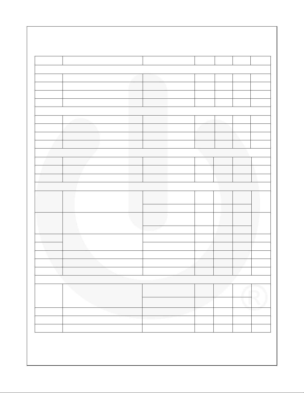
Electrical Characteristics
For typical values, TA=25°C, VIN=15V, and -25°C ≤ TA ≤ 85°C, unless otherwise specified. Specifications to -25°C ~
85°C are guaranteed by design based on final characterization results.
Symbol Parameter Test Conditions Min. Typ. Max. Unit
Under-Voltage Lockout Section (UVLO)
Vth Start Threshold Voltage Increase VIN 4.9 5.2 5.5 V
V
Start Threshold Voltage Hysteresis Decrease VIN 0.20 0.45 0.60 V
thhys
Ist Startup Current VIN=4.5V 10 70 100 µA
Iop Operating Supply Current VIN=15V, Not Switching 0.5 2.0 3.5 mA
ON/OFF Section
Von On-State Input Voltage 1.4 5.0 V
V
Off-State Input Voltage 0.7 V
off
Isb Standby Current ENA=0V 50 120 190 µA
R
Pull-Down Resistor ENA=2V 120 200 280 kΩ
ENA
Reference Section (Recommend 1µF X7R Capacitor)
V5 5V Regulation Voltage 4.9 5.0 5.1 V
FAN7318 — LCD Backlight Inverter Drive IC
V
5V Line Regulation
5line
V
5V Load Regulation
5load
Oscillator Section (Main)
f
Oscillation Frequency
osc
f
Oscillator Frequency in Striking Mode
str
I
ctdcs
I
ctdc
I
ctcs
V
V
cth
ctl
CT Discharge Current
Normal 770 870 970 µA
CT Charge Current Striking -15 -12 -9 µA
CT High Voltage 2 V
CT Low Voltage 0.45 V
Oscillator Section (Burst)
f
Burst Oscillation Frequency
oscb
I
BCT Discharge current 20 26 32 µA
bctdc
V
BCT High Voltage 2 V
bcth
V
BCT Low Voltage 0.5 V
bctl
6 ≤ VIN ≤ 30V
10µA ≤ I
T
A
≤ 3mA
5
=25°C, CT=220pF,
RT=100kΩ
4 50 mV
4 50 mV
101.3 105.0 108.3
kHz
CT=220pF, RT=100kΩ 101 105 109
=25°C, CT=220pF,
T
A
RT=100kΩ
127.5 132.0 136.5
kHz
CT=20pF, RT=100kΩ 127 132 137
Striking 1.03 1.18 1.33 mA
=25°C, BCT=4.7nF,
T
A
BRT=1.4MΩ
BCT=4.7nF,
BRT=1.4MΩ
324 333 345
Hz
320 333 346
© 2009 Fairchild Semiconductor Corporation www.fairchildsemi.com
FAN7318 • 1.0.2 6
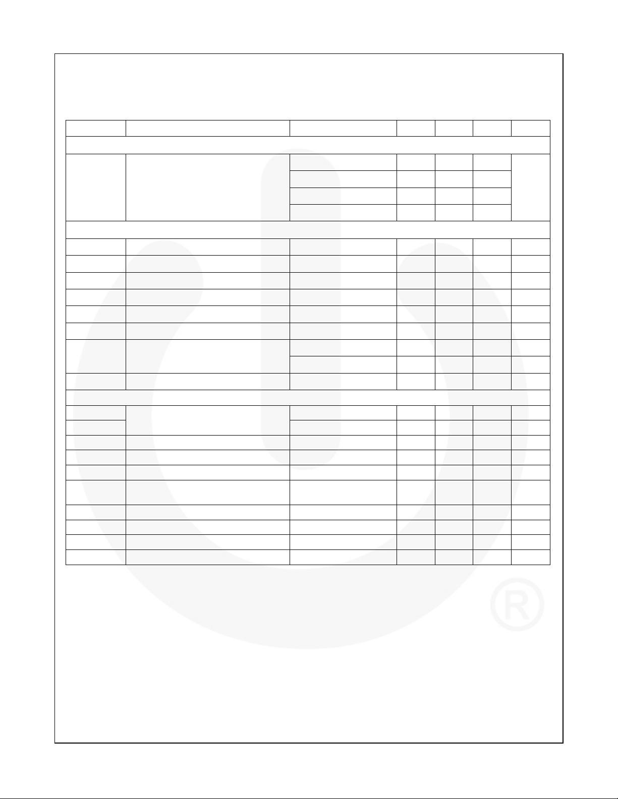
FAN7318 — LCD Backlight Inverter Drive IC
Electrical Characteristics
(Continued)
For typical values, TA=25°C, VIN=15V, and -25°C ≤ TA ≤ 85°C, unless otherwise specified. Specifications to -25°C ~
85°C are guaranteed by design based on final characterization results.
Symbol Parameter Test Conditions Min. Typ. Max. Unit
Analog Dimming Section
ADIM=0V, T
ADIM=0V 1.212 1.310 1.408
AV
Reference Voltage
rexx
ADIM=0.5V 1.16
ADIM=1.0V 0.99
Error Amplifier Section
l
Output Sink Current OLP=2.5V, ADIM=2.5V 63 76 94 µA
sin
l
Output Source Current 1 OLP=0V, ADIM=0V -65 -50 -35 µA
sur1
l
Output Source Current 2 CMP=3V -1.7 -1.3 -0.9 µA
sur2
I
Burst CMP Sink Current BDIM=5V, BCT=0V 41 52 63 µA
bsin
I
OLP Input Current
olpi
I
OLP Output Current OLP=-2V -30 -20 -10 µA
olpo
OLP=2V 0 µA
OLP=0.3V 0.31 V
V
Rectifiers Output of OLP
lpfx
V
OLP Input Voltage Range
olpr
(3)
-4 4 V
OLP=1.5V 1.5 V
Open-Lamp Regulation Section
I
G
olr1
I
olr2
V
olr1
V
olr2
V
olr3
mOLR
I
ors
I
olri
I
olro
V
olrr
Error Amplifier Source Current for
Open-Lamp Regulation
OLR Sweep 0 µA
Open-Lamp Regulation Voltage 1 OLR Sweep 1.24 1.34 1.44 V
Open-Lamp Regulation Voltage 2 Striking, OLR Sweep 1.88 1.98 2.08 V
Open-Lamp Regulation Voltage 3 2.1 2.2 2.3 V
OLR Error Amplifier
Trans-conductance
OLR Error Amplifier Sink Current Normal, OLR=2.5V 50 70 90 µA
OLR Input Current OLR=2.5V 0 µA
OLR Output Current OLR=-2.5V -35 -25 -15 µA
OLR Input Voltage Range
(3)
-4 4 V
Striking, OLR=1.6V -4.0 -3.4 -2.9 µA
180 310 440 µmho
Note:
3. These parameters, although guaranteed, are not 100% tested in production.
=25°C 1.225 1.310 1.402
A
V
© 2009 Fairchild Semiconductor Corporation www.fairchildsemi.com
FAN7318 • 1.0.2 7

FAN7318 — LCD Backlight Inverter Drive IC
Electrical Characteristics
(Continued)
For typical values, TA=25°C, VIN=15V, and -25°C ≤ TA ≤ 85°C, unless otherwise specified. Specifications to -25°C ~
85°C are guaranteed by design based on final characterization results.
Symbol Parameter Test Conditions Min. Typ. Max. Unit
Protection Section
V
Open-Lamp Protection Voltage 0
olp0
V
Open-Lamp Protection Voltage 1 Sweep OLP 0.42 0.49 0.56 V
olp1
V
CMP-High Protection Voltage Sweep CMP 3.4 3.5 3.6 V
cmpr
V
High-FB Protection Voltage
hfbp
V
Short-Lamp Protection Voltage Sweep TIMER 0.22 0.30 0.38 V
slp
V
Timer Threshold Voltage 1 Striking, Sweep TIMER 2.87 3.02 3.17 V
tmr1
V
Timer Threshold Voltage 2 Sweep TIMER 1.0 1.1 1.2 V
tmr2
I
Timer Current 1 OLP=0V 1.7 2.1 2.5 µA
tmr1
I
Timer Current 2 OLR=1.8V 40 50 60 µA
tmr2
TSD Thermal Shutdown
V
Over-Voltage Protection Voltage Sweep OLR 1.24 1.34 1.44 V
ovp
dcr
ENA2.3V OLP Disable/Enable Change
Voltage
(4)
150 °C
Output Section
V
PMOS Gate High Voltage
pdhv
V
PMOS Gate Low Voltage VIN=15V VIN-9.5 VIN-8.5 VIN-7.0 V
phlv
V
NMOS Gate High Voltage VIN=15V 8.0 9.0 10.5 V
ndhv
V
NMOS Gate Low Voltage
ndlv
V
V
I
pdsur
I
pdsin
I
ndsur
I
ndsin
puv
nuv
PMOS Gate Voltage with UVLO
Activated
NMOS Gate Voltage with UVLO
Activated
PMOS Gate Drive Source Current
PMOS Gate Drive Sink Current
NMOS Gate Drive Source Current
NMOS Gate Drive Sink Current
(4)
Maximum / Minimum Duty Cycle
DC
Minimum Duty Cycle
MIN
DC
Maximum Duty Cycle
MAX
(4)
f
(4)
f
Note:
4. These Parameters, although guaranteed, are not 100% tested in production.
(4)
Striking 0.65 0.70 0.75 V
(4)
3.4 3.5 3.6 V
2.1 2.3 2.5 V
(4)
VIN=15V VIN V
VIN=15V 0 V
=4.5V VIN-0.3 V
V
IN
V
=4.5V 0.3 V
IN
(4)
VIN=15V -300 mA
(4)
VIN=15V 400 mA
(4)
VIN=15V 300 mA
(4)
VIN=15V -400 mA
=100kHz 0 %
osc
=100kHz 45 49 %
osc
© 2009 Fairchild Semiconductor Corporation www.fairchildsemi.com
FAN7318 • 1.0.2 8
 Loading...