

Fairchild (Now ON) BSS138W Schematic [ru]
December 2010
BSS138W
N-Channel Logic Level Enhancement Mode Field Effect Transistor
BSS138W — N-Channel Logic Level Enhancement Mode Field Effect Transistor
General Description
These N-Channel enhancement mode field effect
transistor. These products have been designed to
minimize on-state resistance while provide rugged,
reliable, and fast switching performance.These products are particularly suited for low voltage, low current
applications such as small servo motor control, power
MOSFET gate drivers, and other switching applications.
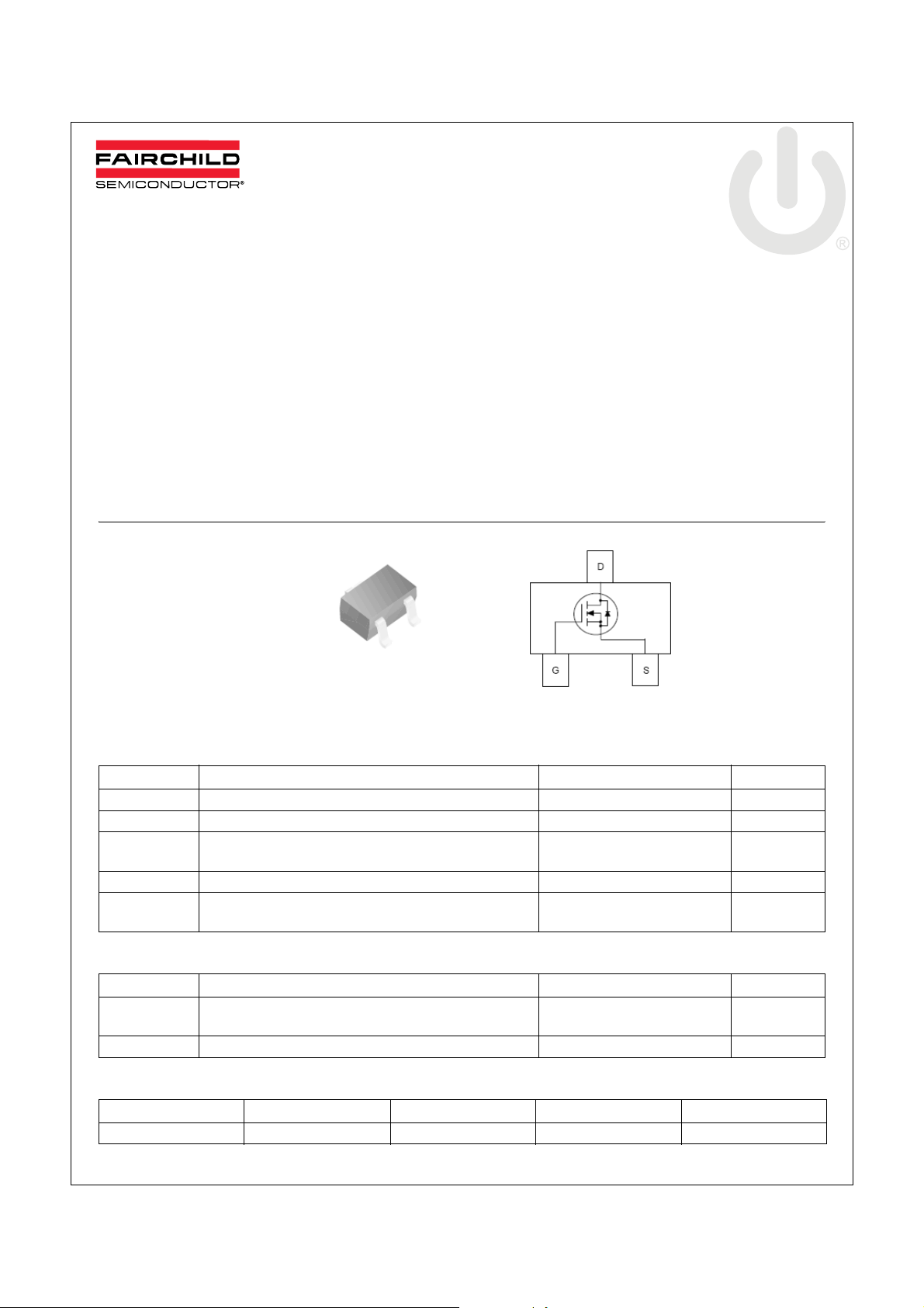
D
G
SOT-323
Marking : 138
Absolute Maximum Ratings T
= 25°C unless otherwise noted
A
S
Features
•R
R
• High density cell design for extremely low R
• Rugged and Reliable
• Compact industry standard SOT-323 surface mount
package
= 3.5Ω @ VGS = 10V, ID = 0.22A
DS(ON)
= 6.0Ω @ VGS = 4.5V, ID = 0.22A
DS(ON)
Symbol Parameter Value Units
V
DSS
V
GSS
I
Drain Current - Continuous (Note1)
D
T
J, TSTG
T
L
Drain-Source Voltage 50 V
Gate-Source Voltage ±20 V
0.21
- Pulsed
Operating and Storage Junction Temperature Range -55 to +150 °C
Maximum Lead Temperature for Soldering
Purposes, 1/16” from Case for 10 Seconds
0.84
300 °C
DS(ON)
A
A
Thermal Characteristics
Symbol Parameter Value Units
P
D
R
θJA
Maximum Power Dissipation (Note1)
Derate Above 25°C
Thermal Resistance, Junction to Ambient (Note1) 367 °C/W
340
2.72
mW
mW/°C
Package Marking and Ordering Information
Device Marking Device Reel Size Tape width Quantity
138 BSS138W 7’’ 8mm 3000 units
© 2010 Fairchild Semiconductor Corporation www.fairchildsemi.com
BSS138W Rev. A0 1
BSS138W — N-Channel Logic Level Enhancement Mode Field Effect Transistor
Electrical Characteristics T
= 25°C unless otherwise noted
A
Symbol Parameter Test Condition Min. Typ. Max. Units
Off Characteristics
BV
ΔBV
ΔT
I
I
DSS
DSS
GSS
Drain-Source Breakdown Voltage V
Breakdown Voltage Temperature
DSS
Coefficient
J
Zero Gate Voltage Drain Current V
Gate-Body Leakage V
= 0V, ID = 250μA50 V
GS
ID = 250μA, Referenced to 25°C71mV/°C
DS
V
DS
V
DS
GS
= 50V, V
= 50V, V
= 30V, V
= ±20V, V
= 0V
GS
= 0V, TJ = 125°C
GS
= 0V
GS
= 0V ±100 nA
DS
0.5
5
100
On Characteristics (Note2)
V
ΔV
R
I
GS(th)
GS(th)
ΔT
DS(ON)
D(ON)
g
FS
Gate Threshold Voltage VDS = VGS, ID = 1mA 0.8 1.3 1.5 V
Gate Threshold Voltage
Temperature Coefficient
J
Static Drain-Source
On-Resistance
On-State Drain Current V
ID = 1mA, Referenced to 25°C-3.9mV/°C
VGS = 10V, ID = 0.22A
= 4.5V, ID = 0.22A
V
GS
VGS = 10V , ID = 0.22A, TJ=125°C
= 10V, V
GS
= 5V 0.2 A
DS
1.17
1.36
2.16
Forward Transconductance VDS = 10V, ID = 0.22A 0.12 S
3.5
6.0
5.8
Dynamic Characteristics
C
C
oss
C
rss
R
Input Capacitance
iss
V
Output Capacitance 5.9 pF
= 25V , V
DS
= 0V , f = 1.0MHz
GS
38 pF
Reverse Transfer Capacitance 3.5 pF
Gate Resistance V
G
= 15mV, f = 1.0MHz 11 Ω
GS
Switching Characteristics (Note2)
t
d(on)
t
t
d(off)
Q
Q
Q
t
Turn-On Delay Time
Turn-On Rise Time 1.9 18
r
Turn-Off Delay Time 6.7 36
Turn-Off Fall Time 6.5 14
f
Total Gate Change
g
Gate-Source Change 0.12
gs
Gate-Drain Change 0.22
gd
VDD = 30V, ID = 0.29A,
V
= 10V, R
GS
= 25V, ID = 0.22A,
V
DS
= 10V
V
GS
GEN
= 6Ω
2.3 5 ns
1.1 nC
Drain-Source Diode Characteristics and Maximum Ratings
I
V
SD
Notes:
1. 367°C/W when mounted on a minimum pad.
2. Pulse Test: Pulse Width ≤ 300μs, Duty Cycle ≤ 2.0%
Maximum Continuous Drain–Source Diode Forward Current 0.22 A
S
Drain-Source Diode Forward
VGS = 0V, IS = 0.44A (Note2) 1.4 V
Voltage
μA
μA
nA
Ω
Ω
Ω
ns
ns
ns
nC
nC
© 2010 Fairchild Semiconductor Corporation www.fairchildsemi.com
BSS138W Rev. A0 2
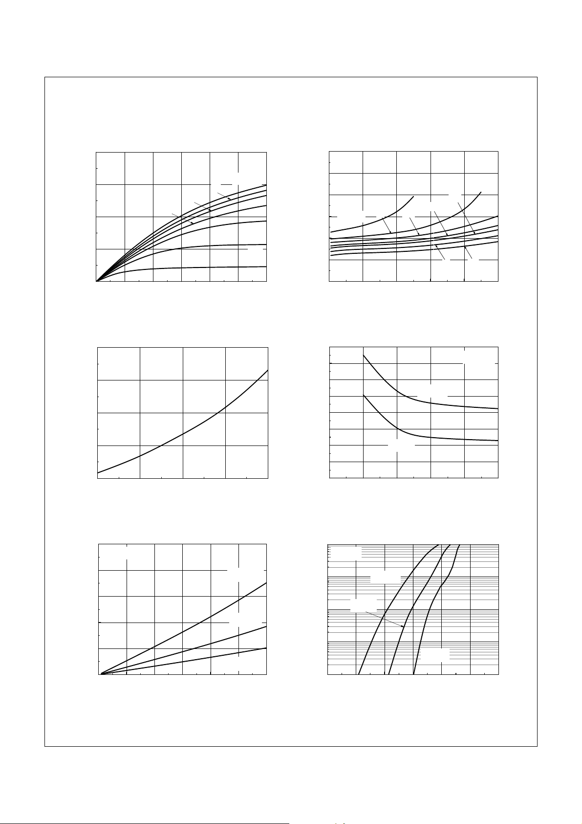
Typical Performance Characteristics
BSS138W — N-Channel Logic Level Enhancement Mode Field Effect Transistor
Figure 1. On-Region Characteristics. Figure 2. On-Resistance Variation with
2.0
1.5
6V
4.5V
1.0
. Drain-Source Current (A)
0.5
D
I
0.0
0.0 0.5 1.0 1.5 2.0 2.5 3.0
3.5V
VDS. Drain-Source Voltage (V)
Figure 3. On-Resistance Variation with
Temperature.
2.5
VGS = 10V
I
= 220 mA
D
2.0
(Ω)
1.5
(on)
DS
R
1.0
Normalized Drain-Source On-Resistance
0.5
-50 0 50 100 150
TJ. Junction Temperature (oC)
VGS = 10V
3V
2.5V
2V
Drain Current and Gate Voltage.
3.5
3.0
2.5
(Ω)
3V
(on),
DS
R
VGS = 2.5V
2.0
1.5
Drain-Source On-Resistance
1.0
0.5
0.00.20.40.60.81.0
3.5V
4.5V
4V
10V
6V
ID. Drain-Source Current(A)
Figure 4. On-Resistance Variation with
Gate-to-Source Voltage.
4.0
3.5
3.0
2.5
(Ω)
2.0
(on)
DS
R
1.5
1.0
Drain-Source On-Resistance
0.5
0.0
0246810
TA = 25oC
TA = 125oC
VGS. Gate to Source Voltage(V)
ID = 110 mA
Figure 5. Drain-Source On Voltage with
Temperature.
2.0
VGS = 10V
1.6
1.2
0.8
. Drain-Source On Volt age ( V )
DS
0.4
V
0.0
0.0 0.1 0.2 0.3 0.4 0.5 0.6
ID. Drain Current (A)
TA = 125(oC)
TA = 25(oC)
TA = -55(oC)
Figure 6. Body Diode Forward Voltage Variation
with Source Current and Temperature.
1000
VGS = 0 V
100
10
1
. Reverse Drain Current [mA]
S
I
0.1
0.0 0.2 0.4 0.6 0.8 1.0 1.2
TA=150oC
TA=25oC
TA=-55oC
VSD. Body Diode Forward Voltage [V]
© 2010 Fairchild Semiconductor Corporation www.fairchildsemi.com
BSS138W Rev. A0 3
 Loading...