Fairchild (Now ON) 1N4148WS, 1N4448WS, 1N914BWS, 1N4148WS, 1N4448WS Schematic [ru]
...
1N4148WS / 1N4448WS / 1N914BWS
Small Signal Diodes
1N4148WS / 1N4448WS / 1N914BWS — Small Signal Diodes
April 2012
Features
• General Purpose Diodes
• Fast Switching Device (T
< 4.0ns)
RR
• Very Small and Thin SMD Package
• Moisture Level Sensitivity 1
• Pb-free Version and RoHS Compliant
• Matte Tin (Sn) Lead Finish
• Green Mold Compound
Absolute Maximum Ratings* T
Symbol
V
RSM
V
RRM
I
FRM
I
O
T
J
T
STG
Non-Repetitive Peak Reverse Voltage 100 V
Repetitive Peak Reverse Voltage 75 V
Repetitive Peak Forward Current 300 mA
Continuous Forward Current 150 mA
Operating Junction Temperature +150 °C
Storage Temperature Range -55 to +150 °C
Parameter Value Units
= 25°C unless otherwise noted
a
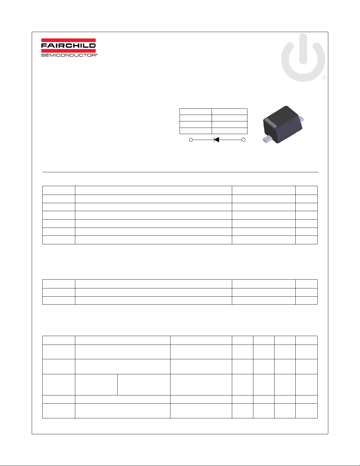
Device Marking Code
Device Type Device Marking
1N4148WS S1
1N4448WS S2
1N914BWS
1. Cathode
ELECTRICAL SYMBOL
S3
2. Anode
1
SOD-323 Flat Lead
Band Indicates Cathode
* These ratings are limiting values above which the serviceability of any semiconductor device may be impaired.
The factory should be consulted on applications involving pulsed or low duty cycle operations.
Thermal Characteristics
2
Symbol
P
D
R
θJA
Power Dissipation (TC = 25°C) 200 mW
Thermal Resistance, Junction to Ambient * 500 °C/W
Parameter Value Units
* Device mounted on FR-4 PCB minimum land pad.
Electrical Characteristics T
Symbol
BV
I
R
V
C
T
RR
© 2012 Fairchild Semiconductor Corporation www.fairchildsemi.com
1N4148WS / 1N4448WS / 1N914BWS Rev. B0 1
Breakdown Voltage IR = 100 μA
R
Reverse Current VR = 20 V
Forward Voltage 1N4448WS/914BWS
F
Diode Capacitance VR = 0, f = 1 MHz 4 pF
O
Reverse Recovery Time IF = 10 mA, IR = 60 mA,
Parameter Test Conditions
1N4148WS
1N4448WS/914BWS
= 25°C unless otherwise noted
a
= 5 μA
I
R
V
= 75 V
R
IF = 5 mA
I
= 10 mA
F
= 100 mA
I
F
= 1 mA, RL = 100 Ω
I
RR
Min. Typ. Max.
100
75
25
5
0.62 0.72
1
1
4ns
Units
V
V
nA
μA
V
V
V

Typical Performance Characteristics
[mA]
]
1N4148WS / 1N4448WS / 1N914BWS — Small Signal Diodes
0.58
0.56
0.54
0.52
0.50
0.48
Capacitance [pF]
0.46
0.44
02468101214
TA=25°C
Reverse Voltage (V)
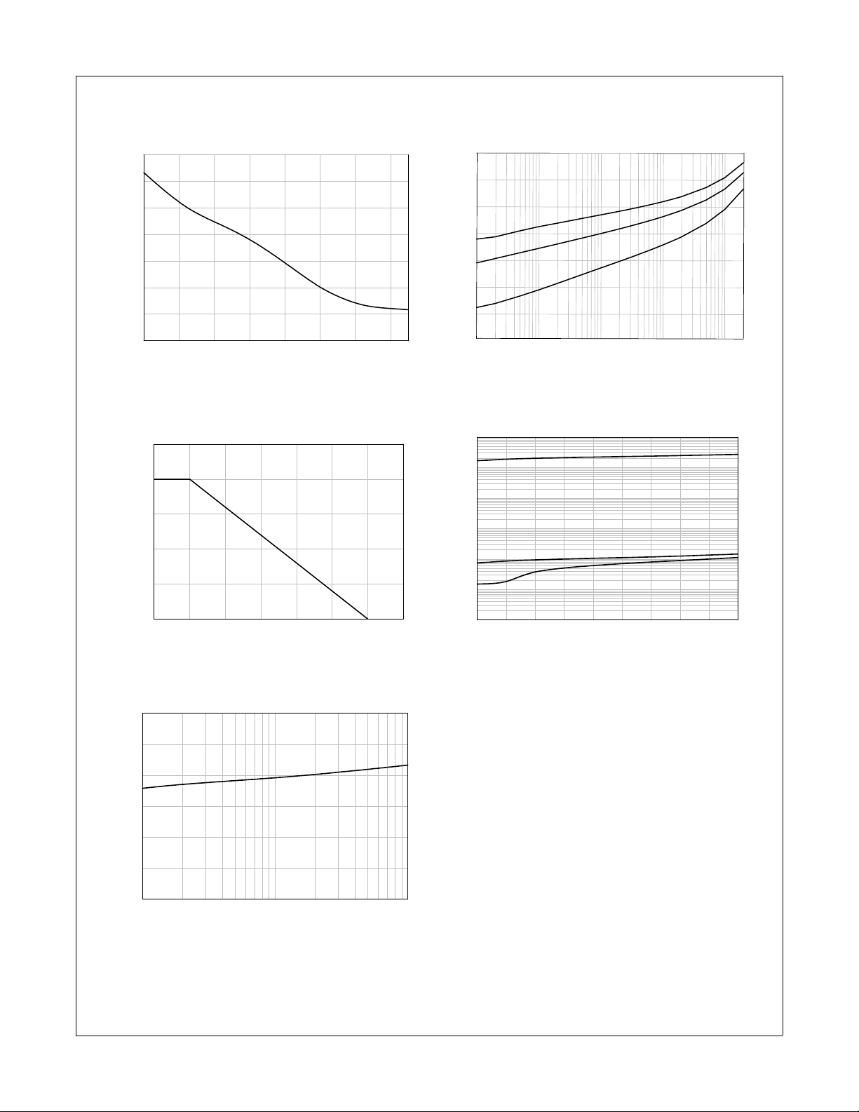
Figure 1. Total Capacitance
250
200
150
100
50
PD - Power Dissipation [mW]
0
0 25 50 75 100 125 150 175
Temperature [°C
Typical
1.2
1.0
0.8
0.6
0.4
Ta=-40°C
Ta=25°C
Ta=150°C
VF- Forward Voltage [V]
0.2
0.0
0.01 0.1 1 10 100
Forward Current, I
F
Figure 2. Forward Voltage vs. Ambient Temperature
5
10
4
10
Ta=150°C
3
10
2
10
Ta=25°C
1
10
Reverse Current [nA]
0
10
Ta=-40°C
-1
10
10 20 30 40 50 60 70 80 90 100
Reverse Voltage, VR[V]
Figure 3. Power Derating Curve Figure 4. Reverse Current vs. Reverse Voltage
170
Ta=25°C
160
150
VR - Reverse Voltage
140
110100
Reverse Current, IR[µA]
Figure 5. Reverse Voltage vs. Reverse Current
© 2012 Fairchild Semiconductor Corporation www.fairchildsemi.com
1N4148WS / 1N4448WS / 1N914BWS Rev. B0 2
 Loading...