

Fairchild USB1T20 service manual
USB1T20
Universal Serial Bus Transceiver
USB1T20 Universal Serial Bus Transceiver
September 2004
Revised January 2005
General Description
The USB1T20 is a generic USB 2.0 compli ant tra nsceiver.
Using a single volta ge supply, the USB1T20 provides an
ideal USB interface solu tion for any electronic devi ce able
to supply 3.0V to 3.6V. It is designed to allo w 5.0 V or 3.3V
programmable and standard logic to interface with the
physical layer of the Universal Ser ial Bus. It is capable of
transmitting and receiving serial data at both full speed
(12Mbit/s) and low speed (1.5Mbi t/s) dat a rate s.
Packaged in industry standard TSSOP and Fairchild’s
ultra-small 2.5mm x 2. 5m m M LP pa ckag e, th e U SB 1T20 is
ideal for ultra-portable electronics and other space constrained applications.
Features
■ Complies with Universal Serial Bus specification 2.0 for
FS/LS applications
■ Utilizes digital inputs and outputs to transmit and receive
USB cable data
■ Supports 12Mbit/s “Full Speed” and 1.5Mbi t/s
“Low Speed” serial data transmission
■ Supports single-end ed and differen tial data inte rface as
function of MODE
■ Single 3. 3V supply
■ ESD Performance: Human Body Model
> 9.5 kV on D−, D+ pins only
> 4 kV on all other pins
■ Space saving 14-terminal MLP package
Ordering Code:
Order Number Package Number Package Description
USB1T20MPX
(Preliminary)
USB1T20MTC
(Note 1)
Note 1: Devices also available in Tape and Reel. Specify by appending th e s uffix let t er “X” to the ordering code.
MLP14D 14-Terminal Molded Leadless Package (MLP), 2.5mm Square
MTC14 14-Lead Thin Shrink Small Outline Package (TSSOP), JEDEC MO-153, 4.4mm Wide
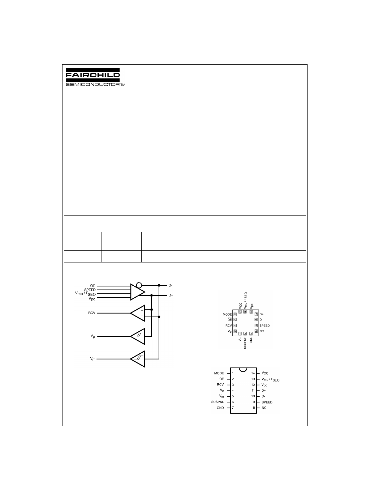
Logic Diagram Connection Diagrams
Te rminal Assignments for MLP (Preliminary)
(Top View)
Pin Assignments for TSSOP
(Top View)
© 2005 Fairchild Semiconductor Corporation DS500894 www.fairchildsemi.com
Terminal and Pin Descriptions
Terminal or Pin
Ter minal or Pin
USB1T20
Name
Number
MLP14D MTC14
RCV 13 3 O Receive data. CMOS level output for USB differential input
OE
12 2 I Output Enable. Active LOW, enables the transceiver to transmit data on the
MODE 11 1 I Mode. When left unconnected, a weak pull-up transistor pulls it to
V
, 8, 9 12, 13 I Inputs to differential driver. (Outputs from SIE).
po
V
/ F
mo
SEO
V
, V
p
m
D
+, D− 7, 6 11, 10 AI/O Data+, Data−. Differential data bus conforming to the Universal Serial Bus
14, 1 4, 5 O Gated version of D− and D+. Outputs are logic “0” and logic “1”. Used to
SUSPND 2 6 I Suspend. Enables a low power state while the USB bus is inactive. While
SPEED 5 9 I Edge rate control. Logic “1” operates at edge rates for “full speed”.
V
CC
10 14 — 3.0V to 3.6V power supply
GND 3 7 — Ground reference
NC 4 8 No Connect
I/O Description
bus. When not active the transceiver is in receive mode.
and in this GND, the Vmo/F
V
CC
(Force SEO).
MODE V
pin takes the function of F
SEO
po
Vmo/F
SEO
000Logic “0”
01SE0
1 0 Logic “1”
11SE0
100SE0
0 1 Logic “0”
1 0 Logic “1”
1 1 Illegal code
detect single ended zero (SE0
), error conditions, and interconnect speed.
(Input to SIE).
V
p
V
m
RESULT
0 0 SE0
0 1 Low Speed
1 0 Full Speed
11Error
standard.
the SUSPND pin is active it will drive the RCV pin to a logic “0” state. Both
+ and D− are 3-STATE.
D
Logic “0” operates edge rates for “low speed”.
SEO
RESULT
Functional Truth Table
Input I/O Outputs
Mode
Vmo/F
V
po
OE SUSPND D+ D− RCV
SEO
V
0 0 0 0 0 0 1 0 0 1 Logic 0
00 1 0000U00SE0
0 1 0 0 0 1 0 1 1 0 Logic 1
01 1 0000U00SE0
10 0 0000U00SE0
1 0 1 0 0 0 1 0 0 1 Logic 0
1 1 0 0 0 1 0 1 1 0 Logic 1
1 1 1 0 0 1 1 U U U Illegal Code
X X X 1 0 ZZUUUD
X X X 1 1 ZZUUUD
X = Don’t Care Z = 3-STATE U = Undefined State
www.fairchildsemi.com 2
V
p
m
Result
+/D− Hi-Z
+/D− Hi-Z
Absolute Maximum Ratings(Note 2) Recommended Operating
DC Supply Voltage (VCC) −0.5V to +7.0V
DC Input Diode Current (I
V
< 0 −50 mA
I
Input Voltage (V
)
I
(Note 3)
Input Voltage (V
I/O
Output Diode Current (I
V
> VCC or VO < 0 ±50 mA
O
Output Voltage (V
(Note 3)
Output Source or Sink Current (I
V
, RCV Pins
p.Vm
= 0V to V
V
O
CC
Output Source or Sink Current (I
D
+/D− Pins
= 0V to V
V
O
V
or GND Current (ICC, I
CC
CC
Storage Temperature (T
)
IK
−0.5V to +5.5V
) −0.5V to VCC + 0.5V
)
OK
)
O
)
O
−0.5V to V
CC
+ 0.5V
±15 mA
)
O
±50 mA
) ±100 mA
GND
) −60°C to + 150°C
STO
Conditions
Supply Voltage V
Input Voltage (V
Input Range for AI/O (V
Output Voltage (VO)0V to V
Operating Ambient Temperature
in Free Air (T
Note 2: The Absolute Maxi mum Ratings are thos e values beyond which
the safety of the d evice cannot b e guaranteed . The device sh ould not be
operated at these limit s. The parametric values defi ned in the Electrical
Characteristic tables are not guaranteed at the absolute maximum rating.
The “Recomm ended O peratin g Cond itions ” table will defin e the condition s
for actual device operation.
Note 3: The input and output voltage ratings may be exceeded if the input
and output clamp current ratings are observed.
CC
) 0V to 5.5V
I
AMB
)0V to V
AI/O
) −40°C to +85°C
DC Electrical Characteristics (Digital Pins)
Over recommended range of supply voltage and operating free air temperature (unless otherwise noted). VCC = 3.0V to 3.6V
Symbol Parameter Test Conditions
Input Levels
V
IL
V
IH
Output Levels
V
OL
V
OH
Leakage Current
I
L
I
CCFS
I
CCLS
I
CCQ
I
CCS
LOW Level Input Voltage 0.8 V
HIGH Level Input Voltage 2.0 V
LOW Level Output Voltage IOL = 4 mA 0.4
HIGH Level Output Voltage IOH = 4 mA 2.4
Input Leakage Current VCC = 3.0 to 3.6 ±5 µA
Supply Current (Full Speed) VCC = 3.0 to 3.6 5 mA
Supply Current (Low Speed) VCC = 3.0 to 3.6 5 mA
Quiescent Current VCC = 3.0 to 3.6
Supply Current in Suspend VCC = 3.0 to 3.6; Mode = V
IOL = 20 µA0.1
= 20 µAV
I
OH
VIN = VCC or GND
CC
Min Typ Max
CC
Limits
– 0.1
USB1T20
3.0V to 3.6V
CC
CC
UnitTemperature = −40°C to +85°C
V
V
5mA
10 µA
3 www.fairchildsemi.com
 Loading...