查询USB1T11A供应商
USB1T11A
Universal Serial Bus Transceiver
USB1T11A Universal Serial Bus Transceiver
November 1999
Revised March 2005
General Description
The USB1T11A is a one chip generic USB transceiver. It is
designed to allow 5.0V o r 3.3V programmable and standard logic to interfac e with the physical layer of the Universal Serial Bus. It is capable of transmitting an d receiving
serial data at both full speed (12Mbit/s) and low speed
(1.5Mbit/s) data rates.
The input and output signals of the USB1T11A conform
with the “Seria l Interface Engine”. Implementati on of the
Serial Interface Engine along with the USB1T11A allows
the designer to make US B com pati ble de vices w ith off-th eshelf logic and easily modify and update the application.
Features
■ Complies with Universal Serial Bus specification 1.1
■ Utilizes digital inputs and outputs to transmit and receive
USB cable data
■ Supports 12Mbit/s “Full Speed” and 1.5Mbit/s
“Low Speed” serial data transmission
■ Compatible with the VHDL “Serial Interface Engine”
from USB Implementers' Forum
■ Supports single-ended data interface
■ Single 3. 3V supply
■ ESD Performance: Human Body Model
!
9.5 kV on D, D pins only
!
4 kV on all other pins
■ 16-lead Pb-Free MLP package saves space
Ordering Code:
Order Number
USB1T11AM
(Note 1)
USB1T11AM_NL
(Note 2)
USB1T11ABQX MLP16C Pb-Free 16-Terminal Molded Leadless Package (MLP), JEDEC MO-220, 3mm square
USB1T11AMTC
(Note 1)
USB1T11AMTC_NL
(Note 2)
USB1T11AMTCX_NL
(Note 2)
Pb-Free package per JEDEC J-STD-020B.
Note 1: Device also available in Tape and Reel. Specify by appending suffix letter “X” to the ordering code.
Note 2: “_NL” indicates Pb-Fre e pac k age (per JEDEC J-ST D-020B). Please us e order number as indi c at ed.
Package
Number
M14A 14-Lead Small Outline Integrated Circuit (SOIC), JEDEC MS-012, 0.150" Narrow
M14A Pb-Free 14-Lead Small Outline Integrated Circuit (SOIC), JEDEC MS-012, 0.150" Narrow
MTC14 14-Lead Thin Shrink Small Outline Package (TSSOP), JEDEC MO-153, 4.4mm Wide
MTC14 Pb-Free 14-Lead Thin Shrink Small Outline Package (TSSOP), JEDEC MO-153, 4.4mm
Wide
MTC14 Pb-Free 14-Lead Thin Shrink Small Outline Package (TSSOP), JEDEC MO-153, 4.4mm
Wide
Package Description
The USB-IF Logos ar e trademarks of Unive rs al Serial Bus Implem enters Forum, Inc.
© 2005 Fairchild Semiconductor Corporation DS500234 www.fairchildsemi.com

Connection Diagrams
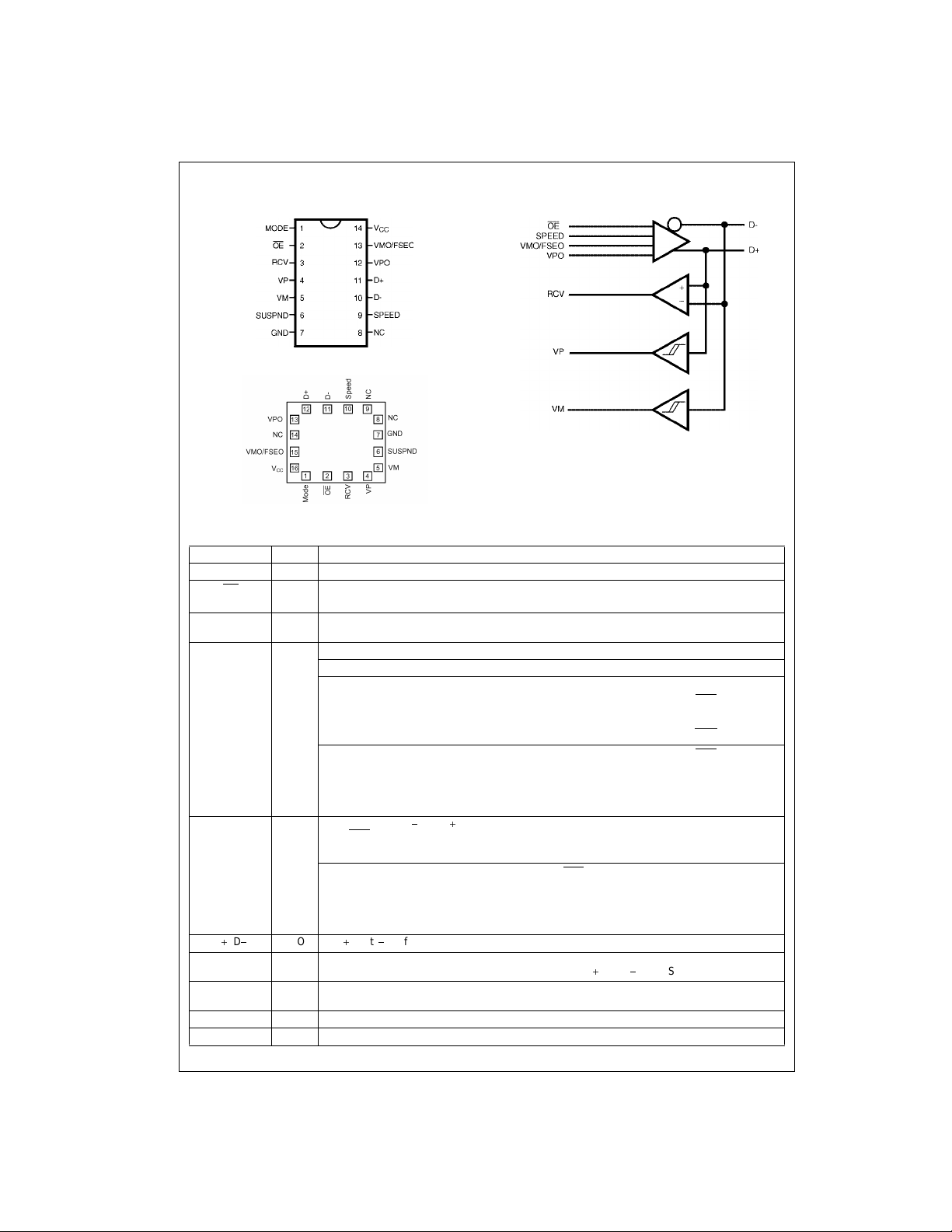
Pin Assignments for SOIC and TSSOP
Logic Diagram
USB1T11A
Pin Assignments for MLP
Pin Descriptions
Pin Name I/O Description
RCV O Receive data. CMOS level output for US B differen tial input
OE
MODE I Mode. When left unconnected, a weak pull-up transistor pulls it to V
, VMO/F
V
PO
, V
V
P
M
, D
D
SUSPND I Suspend. Enables a low power state while the USB bus is inactive. While the suspend pin is
SPEED I Edge rate control. Logic “1” operates at edge rates for “full speed”.
V
CC
GND Ground reference
I Output Enable. Active LOW, enables the transceiver to transmit data on the bus. When not
active the transceiver is in receive mode.
and in this GND, the
VMO/FSEO pin takes the function of FSEO (Force SEO).
I Inputs to differential driver. (Outputs from SIE).
SEO
O Gated versi on of D and D. Outputs are logic “0” and logic “1”. Used to detect single ended
AI/O Data, Data. Differential data bus conforming to the Universal Serial Bus standard.
MODE VPO VMO/FSEO RESULT
0 0 0 Logic “0”
0 1 SE0
1 0 Logic “1”
11 SEO
1 0 0 SE0
0 1 Logic “0”
1 0 Logic “1”
1 1 Illegal code
zero (SE0
active it will drive the RCV pin to a logic “0” state. Both D
Logic “0” operates edge rates for “low speed”.
3.0V to 3.6V power supply
), error conditions, and interconnect speed. (Input to SIE).
VP VM RESULT
0 0 SE0
01Low Speed
1 0 Full Speed
11Error
CC
and D are 3-STATE.
www.fairchildsemi.com 2

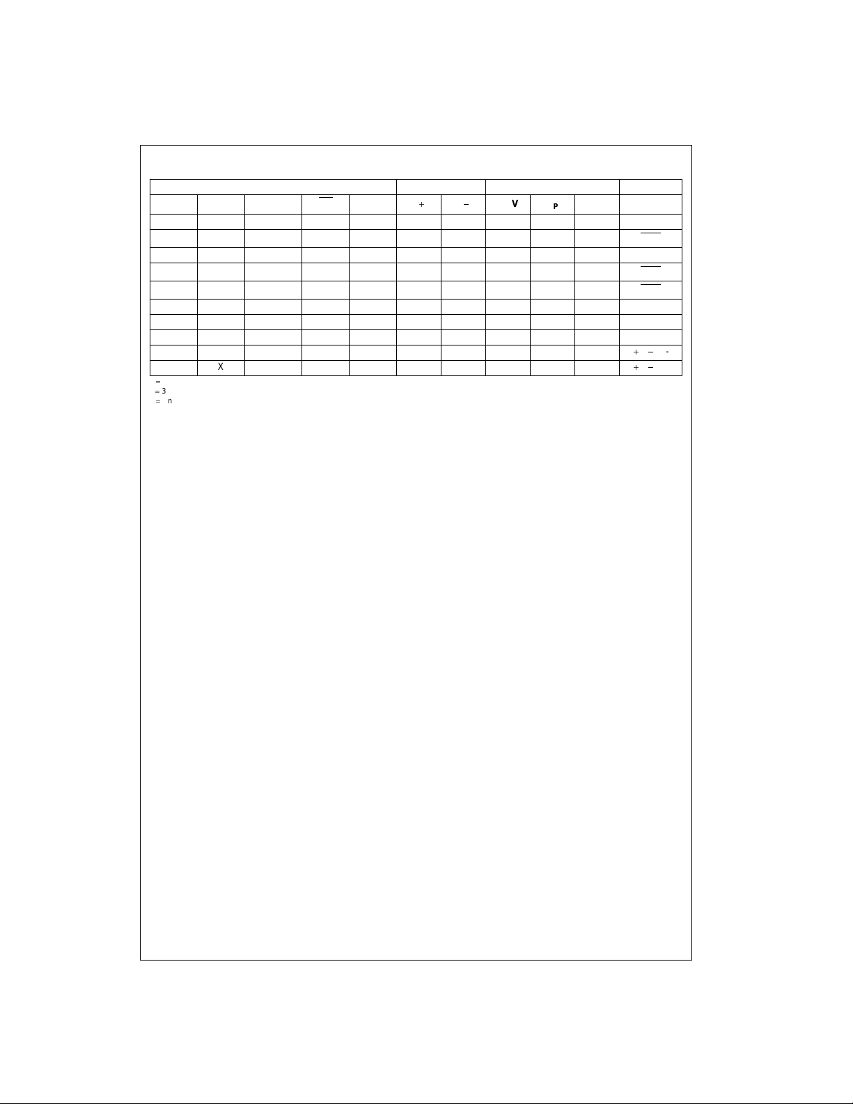
Functional Truth Table
Input I/O Outputs
Mode VPO VMO/FSEO OE
SUSPND D
D
RCV
V
0 0 0 0 0 0 1 0 0 1 Logic 0
0 0 1 0 0 0 0 U 0 0 SEO
0 1 0 0 0 1 0 1 1 0 Logic 1
0 1 1 0 0 0 0 U 0 0 SEO
1 0 0 0 0 0 0 U 0 0 SEO
1 0 1 0 0 0 1 0 0 1 Logic 0
1 1 0 0 0 1 0 1 1 0 Logic 1
1 1 1 0 0 1 1 U U U Illegal Code
XX X 10ZZUUUD
XX X 11ZZUUUD
X Don’t Care
Z
3-STATE
Undefined State
U
V
P
M
Result
/D
/D
USB1T11A
Hi-Z
Hi-Z
3 www.fairchildsemi.com

Absolute Maximum Ratings(Note 3) Recommended Operating
DC Supply Voltage (VCC)
DC Input Diode Current (I
V
0
USB1T11A
I
Input Voltage (V
)
I
(Note 4)
Input Voltage (V
)
I/O
Output Diode Current (I
! VCC or VO 0
V
O
Output Voltage (V
O
(Note 4)
Output Source or Sink Current (I
VP.VM, RCV pins
0 to V
V
O
CC
Output Source or Sink Current (I
D
/D
pins
0 to V
V
O
V
CC
CC
or GND Current (ICC, I
Storage Temperature (T
0.5V to 7.0V
)
OK
IK
0.5V to VCC 0.5V
)
50 mA
0.5V to 5.5V
r
50 mA
)
0.5V to VCC 0.5V
)
O
r
15 mA
)
O
r
50 mA
STO
GND
)
)
60q
C to 150qC
r
100 mA
Conditions
Supply Voltage V
Input Voltage (V
Input Range for AI/O (V
Output Voltage (VO) 0V to V
Operating Ambient Temperature
in free air (T
Note 3: The Absolute Maximum Ratings are those values beyond which
the safety of the d evice cannot be guaranteed. The device sh ould not be
operated at these limi ts. The parametric values define d in the Electrical
Characteristic tables are not gua ranteed at the absolute ma ximum rating .
The “Recomme nded O peratin g Cond itions ” table w ill def ine th e cond itions
for actual device operation.
Note 4: The input and o utp ut vol tage r ati ngs ma y be ex ceed ed if th e inpu t
and output clamp c urrent ratings are observ ed.
CC
)0V to 5.5V
I
amb
) 0V to V
AI/O
)
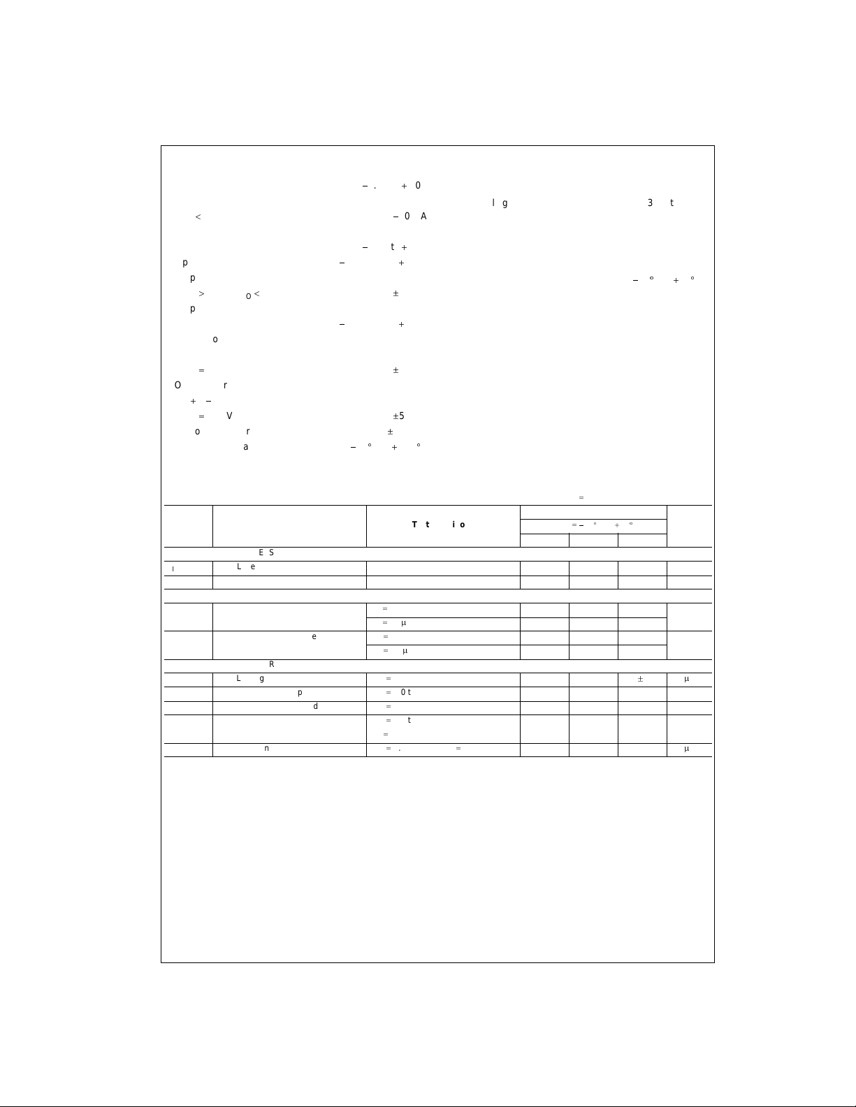
DC Electrical Characteristics (Digital Pins)
Over recommended range of supply voltage and operating free air temperature (unless otherwise noted). VCC 3.0V to 3.6V
Symbol Parameter Test Conditions
Min Typ Max
CC
V
V
V
V
I
L
I
CCFS
I
CCLS
I
CCQ
I
CCS
INPUT LEVELS:
IL
IH
OL
OH
LOW Level Input Voltage 0.8 V
HIGH Level Input Voltage 2.0 V
OUTPUT LEVELS:
LOW Level Output Voltage IOL 4 mA 0.4
HIGH Level Output Voltage IOH 4 mA 2.4
LEAKAGE CURRENT:
Input Leakage Current VCC 3.0 to 3.6
Supply Current (Full Speed) VCC 3.0 to 3.6 5 mA
Supply Current (Low Speed) VCC 3.0 to 3.6 5 mA
Quiescent Current VCC 3.0 to 3.6
Supply Current in Suspend VCC 3.0 to 3.6; Mode V
IOL 20 PA0.1
20 PAV
I
OH
VIN VCC or GND
CC
Limits
– 0.1
3.0V to 3.6V
CC
CC
40q
C to 85qC
UnitTemp 40qC to 85qC
V
V
r
5
P
A
5mA
10
P
A
www.fairchildsemi.com 4
 Loading...