查询USB1T1104供应商
USB1T1104
Universal Serial Bus Peripheral Transceiver
with Voltage Regulator
USB1T1104 Universal Serial Bus Peripheral Transceiver with Voltage Regulator
August 2004
Revised August 2005
General Description
The USB1T1104 is an Universal Serial Bus Specification Rev
2.0 compliant transceiver. The device provides an USB interface for Full-Speed (12Mbit/s) USB applications. The
USB1T1104 provides excellent flexibility, allowing differential
and single ended inputs while an integrated voltage regulator
sets the I/O level to 1.65V to 3.6V . Utilizing an integrated 5.0V to
3.3V voltage regulator, the part can be powered directly from
the USB host (V
local sources while used in devices with low supply voltages.
The USB1T1104 provides 15kV ESD protection on the USB bus
pins (D
/D
devices while providing excellent protection to larger and more
expensive ASICs and USB controllers.
) to minimize the power consumed from the
BUS
). This eliminates the need for any external ESD
Features
O
Complies with Universal Serial Bus Specification 2.0
O
Integrated 5V to 3.3V voltage regulator for powering VBus
O
Utilizes digital inputs and outputs to transmit and receive USB
cable data
O
Supports full speed 12Mbits/s speed data rates
O
Ideal for portable electronic devices
O
15kV contact HBM ESD protection on bus pins
O
3.3mm leadless package
O
Industry standard HBCC footprint is lead-free
Applications
O
Cell phone
O
Digital camera
O
MP3
Ordering Code:
Order Package
Number Number
USB1T1104MHX MLP16HB Pb-Free 16-Terminal Molded Leadless Package (MHBCC), JEDEC MO-217, 3mm Square
Package Description
Pb-Free package per JEDEC J-STD-020B.
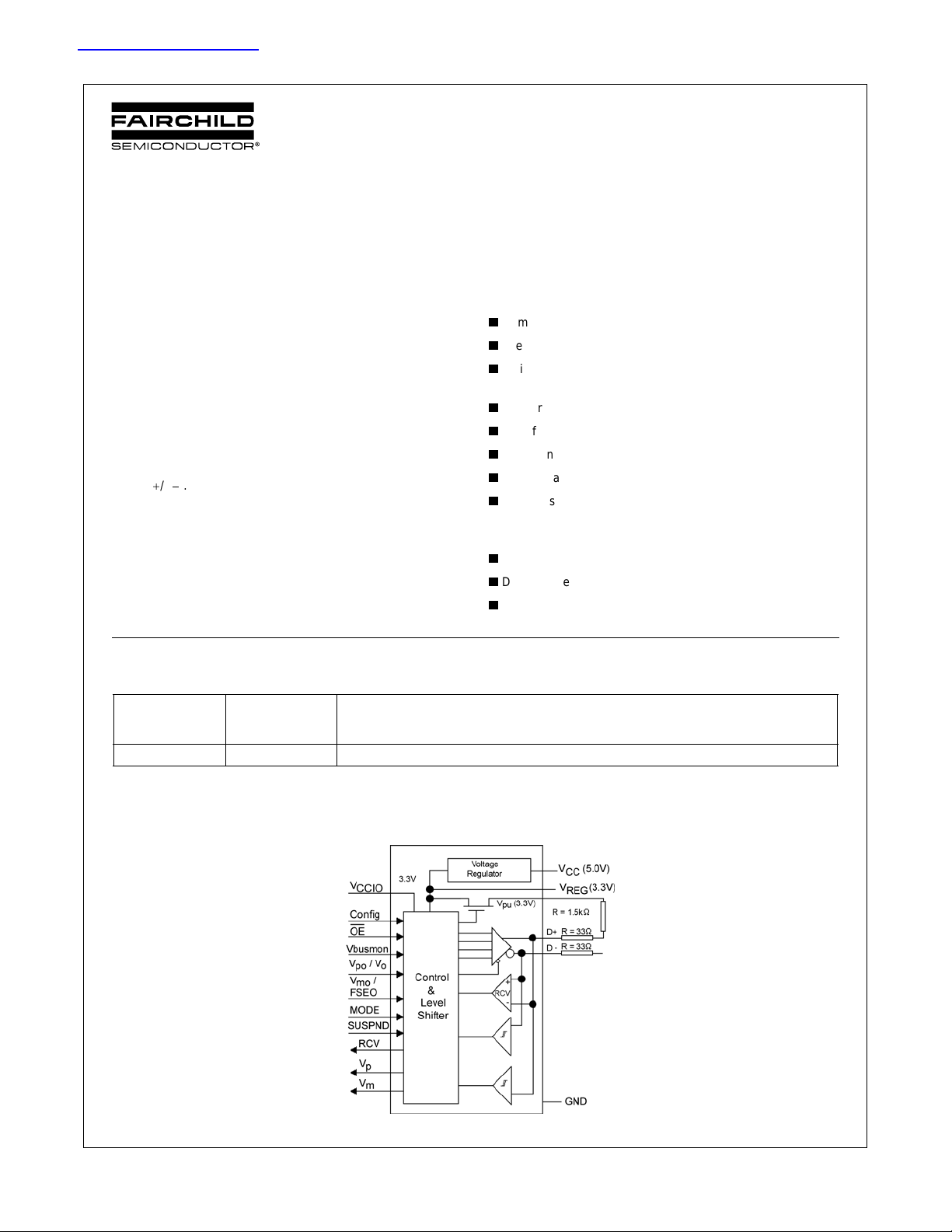
Logic Diagram
© 2005 Fairchild Semiconductor Corporation DS500893 www.fairchildsemi.com

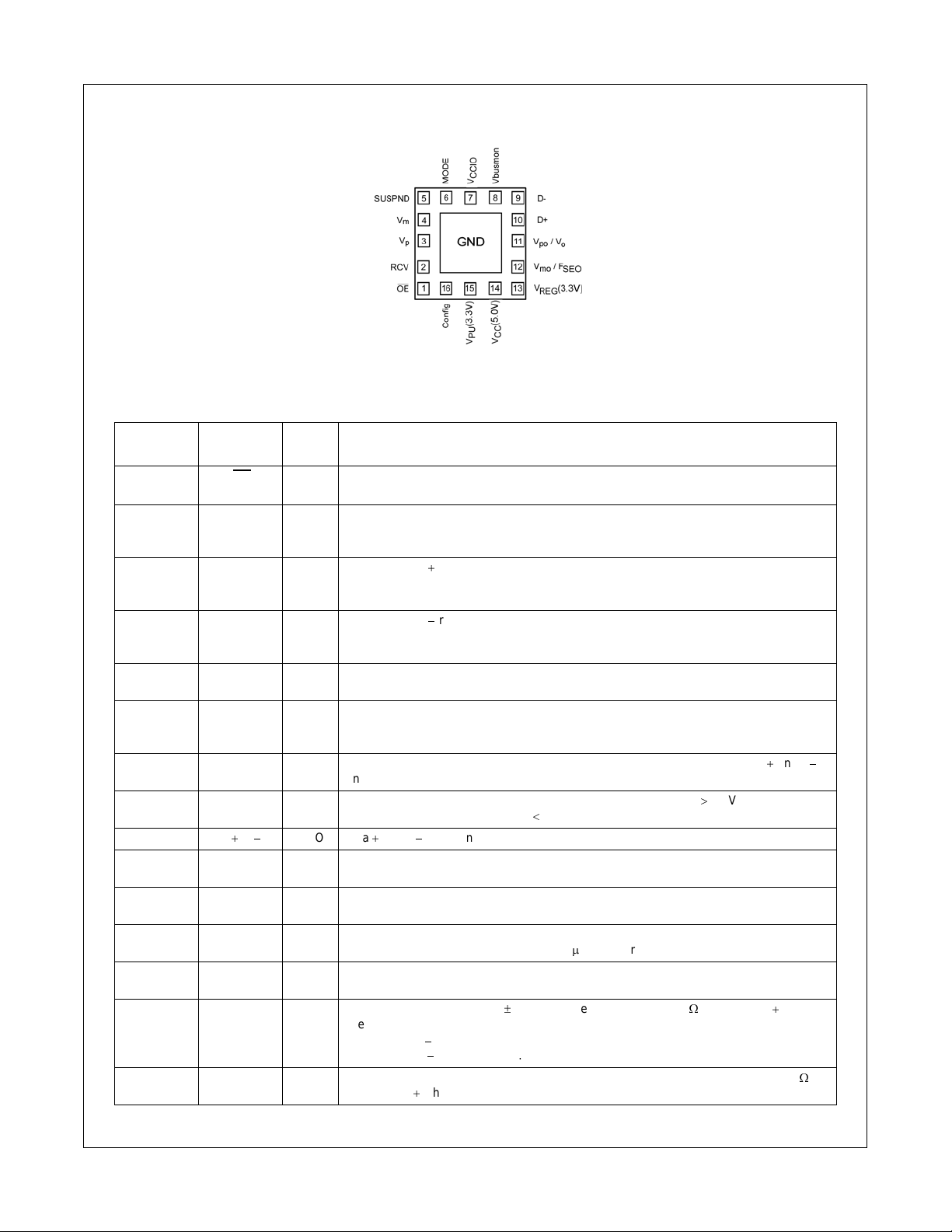
Connection Diagram
USB1T1104
Terminal Descriptions
(Bottom View)
Terminal
Number
Terminal
Name
I/O Terminal Description
1OEI Output Enable: Active LOW enables the transceiver to transmit data on the bus. When not
active the transceiver is in the receive mode (CMOS level is relative to V
CCIO
)
2 RCV O Receive Data Output: Non-inverted CMOS level output for USB differential Input (CMOS
3V
4V
p
m
output level is relative to V
and preserved during SE0 condition.
O Single-ended D receiver output VP (CMOS level relative to V
detection of SEO, error conditions, speed of connected device; Driven HIGH when no
supply connected to V
O Single-ended D receiver output Vm (CMOS level relative to V
). Driven LOW when SUSPN is HIGH; RCV output is stable
CCIO
): Used for external
CCIO
CC
and V
REG
.
): Used for external
CCIO
detection of SEO, error conditions, speed of connected device; Driven HIGH when no
supply connected to V
5 SUSPND I Suspend: Enables a low power state (CMOS level is relative to V
CC
and V
REG
.
).
CCIO
While the SUSPND pin is active (HIGH) it will drive the RCV pin to logic “0” state.
6 MODE I MODE input (CMOS level is relative to V
, Vmo) whereas a LOW enables the single-ended MODE (Vo, V
(V
po
Table 4
7V
CCIO
Supply Voltage for digital I/O pins (1.65V to 3.6V): When not connected the D and D
pins are in 3-STATE. This supply bus is totally independent of V
8 Vbusmon O Vbus monitor output (CMOS level relative to V
3.6V then Vbusmon = LOW.
10, 9 D
11 V
Vbusmon = HIGH and when Vbus
, D
AI/O Data , Data : Differential data bus conforming to the USB standard.
/ V
po
o
I Driver Data Input (CMOS level is relative to V
). A HIGH selects the differential input MODE
CCIO
): When Vbus ! 4.1V then
CCIO
); Schmitt trigger input; see Table 2 and
CCIO
FSEO
(5V) and V
CC
) see T able 2 and
Table 3
12 V
mo
/ F
SEO
I Driver Data Input (CMOS level is relative to V
); Schmitt trigger input; see Table 2 and
CCIO
Table 3
13 V
14 V
15 V
(3.3V) Internal Regulator Option: Regulated supply output voltage (3.0V to 3.6V) during 5V oper-
REG
ation; decoupling capacitor of at least 0.1
(5.0V) Internal Regulator Option: Used as supply voltage input (4.0V to 5.5V); can be connected
CC
(3.3V) Pull-up Supply Voltage (3.3V r 10%): Connect an external 1.5k: resistor on D (FS data
PU
directly to USB line Vbus.
rate); Pin function is controlled by Config input pin:
Config = LOW
Config = HIGH
VPU (3.3V) is floating (High Impedance) for zero pull-up current.
VPU (3.3V) = 3.3V; internally connected to V
P
F is required.
REG
(3.3V).
16 Config I USB connect or disconnect software control input. Configures 3.3V to external 1.5k
resistor on D
when HIGH.
REG
(3.3V).
:
www.fairchildsemi.com 2

USB1T1104
Terminal
Number
Exposed
Diepad
Terminal
Name
GND GND GND supply down bonded to exposed diepad to be connected to the PCB GND.
I/O Terminal Description
Functional Description
The USB1T1104 transceiver is designed to convert CMOS data
into USB differential bus signal levels and to convert USB differential bus signal to CMOS data.
To minimize EMI and noise t he outputs are edge rate controlled
with the rise and fall times controlled and defined for full speed
data rates. The rise, fall times are balanced between the differential pins to minimize skew.
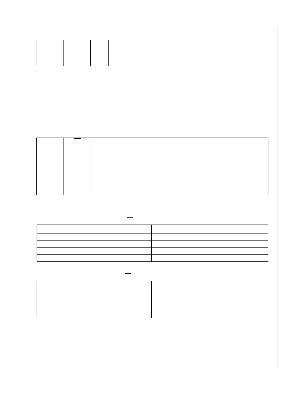
Functional Tables
TABLE 1. Function Select
SUSPND OE D, D RCV
L L Driving &
Receiving
L H Receiving
(Note 1)
H L Driving Inactive
HH3-STATE
(Note 1)
Active Active Normal Driving (Diff erential Receiver Active)
Active Active Receiving
(Note 2)
Inactive
(Note 2)
Table 1 describes the specific pin functionality selection.
Table 2, Table 3, and Table 4 describe the specific Truth Tables
for Driver and Receiver operating functions.
The USB1T1104 also has the capability of various power supply
configurations to support mixed voltage supply applications (see
Table 5) and Power Supply Configurations and Options for
detailed descriptions.
V
p/Vm
Active Driving during Suspend
Active Low Power State
(Differential Receiver Inactive)
Function
Note 1: Signal levels is function of connection and/or pull-up/pull-down resistors.
Note 2: For SUSPND = HIGH mode the differential receiver is inactive and the output RCV output is forced LOW. The out-of-suspend signaling (K) is detected via the single-
ended receiver outputs of the Vp and Vm pins.
TABLE 2. Driv e r Func tion (OE = L) using Differential Input Interface Mode Pin = H
V
mo
L L SE0 (Note 3)
L H Differential Logic 1
H L Differential Logic 0
H H Illegal State
Note 3: SE0 = Single Ended Zero
TABLE 3. Driver Function (OE = L) using Single-ended Input Interface Mode Pin = L
FSE0
L L Differential Logic 0
L H Differential Logic 1
H L SE0 (Note 4)
H H SE0 (Note 4)
Note 4: SE0 = Single Ended Zero
V
po
V
o
Data
Data
3 www.fairchildsemi.com

TABLE 4. Receiver Function (OE = H)
D, D RCV
USB1T1104
X = Don’t Care
Differential Logic 1 H H L
Differential Logic 0 L L H
SE0 X L L
Sharing Mode L H H
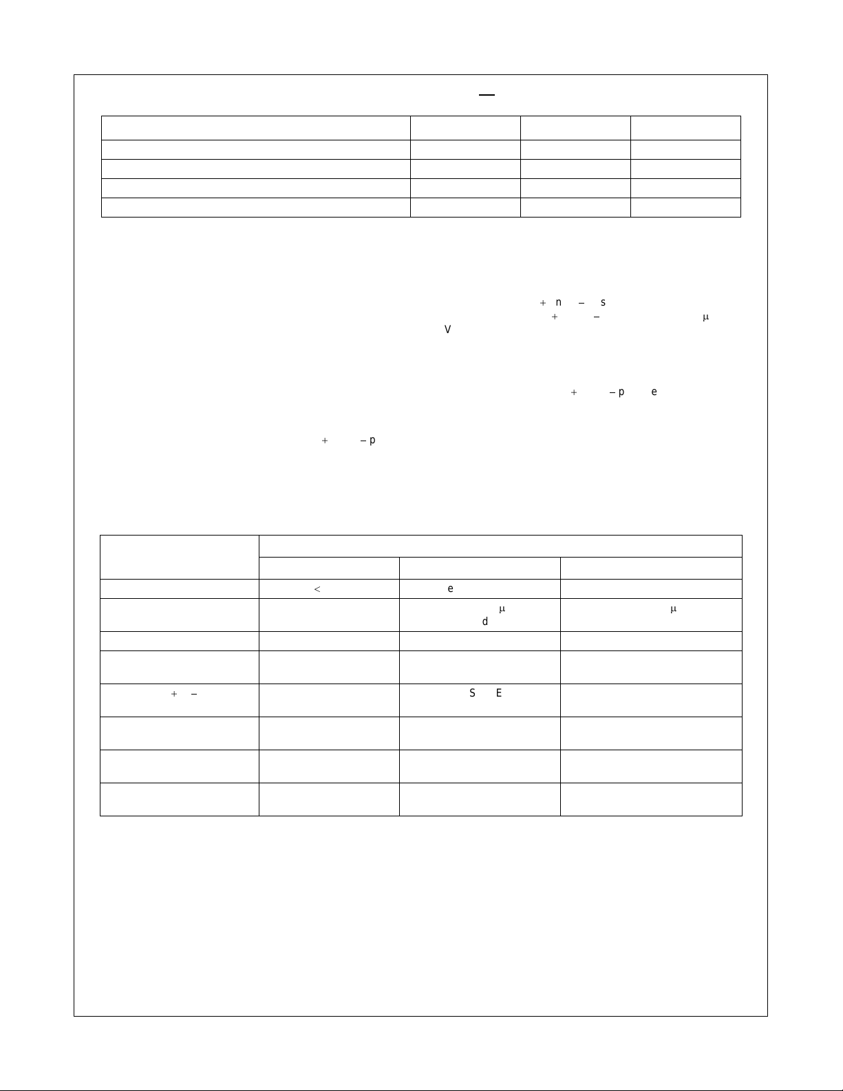
Power Supply Configurations and Options
The three modes of power supply operation are:
• Normal Mode: Regulated Output
1. Regulated Output. V
connected to 5V (4.0V to 5.5V) and the internal voltage
regulator then produces 3.3V for the USB connections.
For normal mode the V
(1.65V to 3.6V) that is a function of the external circuit configuration.
• Sharing Mode: V
V
are not connected. In this mode the D and D pins are
REG
CCIO
is connected and VCC (5.0) is
CCIO
is an independent voltage source
CCIO
is only supply connected. VCC and
TABLE 5. Power Supply Configuration Options
V
p
V
m
3-STATE and the USB1T1104 allows external signals up to
3.6V to share the D
limits leakage from D
such that device is in low power (suspended) state.
V
CCIO
Pins Vbusmon and RCV are forced LOW as an indication of
and D bus lines. Internally the circuitry
and D pins (maximum 10 PA) and
this mode with Vbusmon being ignored during this state.
• Disable Mode: V
nected. In this mode the D
is not connected and VCC(5V) is con-
CCIO
and D pins are 3-STATE and the
device is in low power state.
A summary of the Supply Configurations is described in Table 5.
Pins
V
(5V)
CC
(3.3V) Pulled LOW
V
REG
V
CCIO
V
(3.3V) 3-STATE (Off) 3-STA TE (Off) 3.3V Available if
PU
D
, D
V
, V
p
m
RCV L Invalid Function of
OE, SUSPND, Config,
, Vmo/F
V
po/Vo
Note 5: Hi-Z or forced LOW.
SEO
, MODE
Power Supply Mode Configuration
Sharing Disable Normal (Regulated Output)
3.6V Connected to 5V Source Connected to 5V Source
3.3V, 300 PA
Regulator OFF
Regulated Output
1.65V to 3.6V Source Not Connected 1.65V to 3.6V Source
3-STATE 3-STATE Function of
H Invalid Function of
Hi-Z Hi-Z Function of
3.3V, 300 PA
Regulated Output
Config = HIGH
Mode Set Up
Mode Set Up
Mode Set Up
Mode Set Up
www.fairchildsemi.com 4
 Loading...