Fairchild USB1T1103 service manual
查询USB1T1103供应商
USB1T1103
Universal Serial Bus Peripheral Transceiver
with Voltage Regulator
USB1T1103 Universal Serial Bus Peripheral Transceiver with Voltage Regulator
April 2005
Revised May 2005
General Description
This chip provides a USB Transceiver functionality with a
voltage regulator that is compliant to USB Specification
Rev 2.0. this integrated 5V to 3.3 V regulator allows interfacing of USB Application specific devices with supply voltages ranging from 1.65 V to 3.6V wi th the physica l layer of
Universal Serial Bus. It is capable of operating at 12Mbits/s
(full speed) data rate s and hence is ful ly compl iant to USB
Specification Rev 2.0. The Vbusmon terminal allows for
monitoring the Vbus line.
The USB1T1103 also provides exceptional ESD pro tection
with 15kV contact HBM on D
, D terminals.
Features
■ Complies with Universal Serial Bus Specification 2.0
■ Integrated 5V to 3.3V voltage regulator for powering
VBus
■ Utilizes digital inputs and outputs to transmit and receive
USB cable data
■ Supports full speed (12Mbits/s) data rates
■ Ideal for portable el ectronic devices
■ MLP technology package (16 terminal) with HBCC
footprint
■ 15kV contact HBM ESD protection on bus terminals
■ Supports disable mode and is functionally equivalent to
Philips ISP1102
Applications
•PDA
• PC Peripherals
• Cellular Phones
•MP3 Players
• Digital Still Camera
• Information Appliance
Ordering Code:
Order Number
USB1T1103MPX MLP14D Pb-Free 14-Terminal Molded Leadless Package (MLP), 2.5mm Square
USB1T1103MHX MLP16HB Pb-Free 16-Terminal Molded Leadless Package (MHBCC), JEDEC MO-217, 3mm Square
Pb-Free package per JEDEC J-STD-020B.
Package
Number
Package Description
© 2005 Fairchild Semiconductor Corporation DS500905 www.fairchildsemi.com
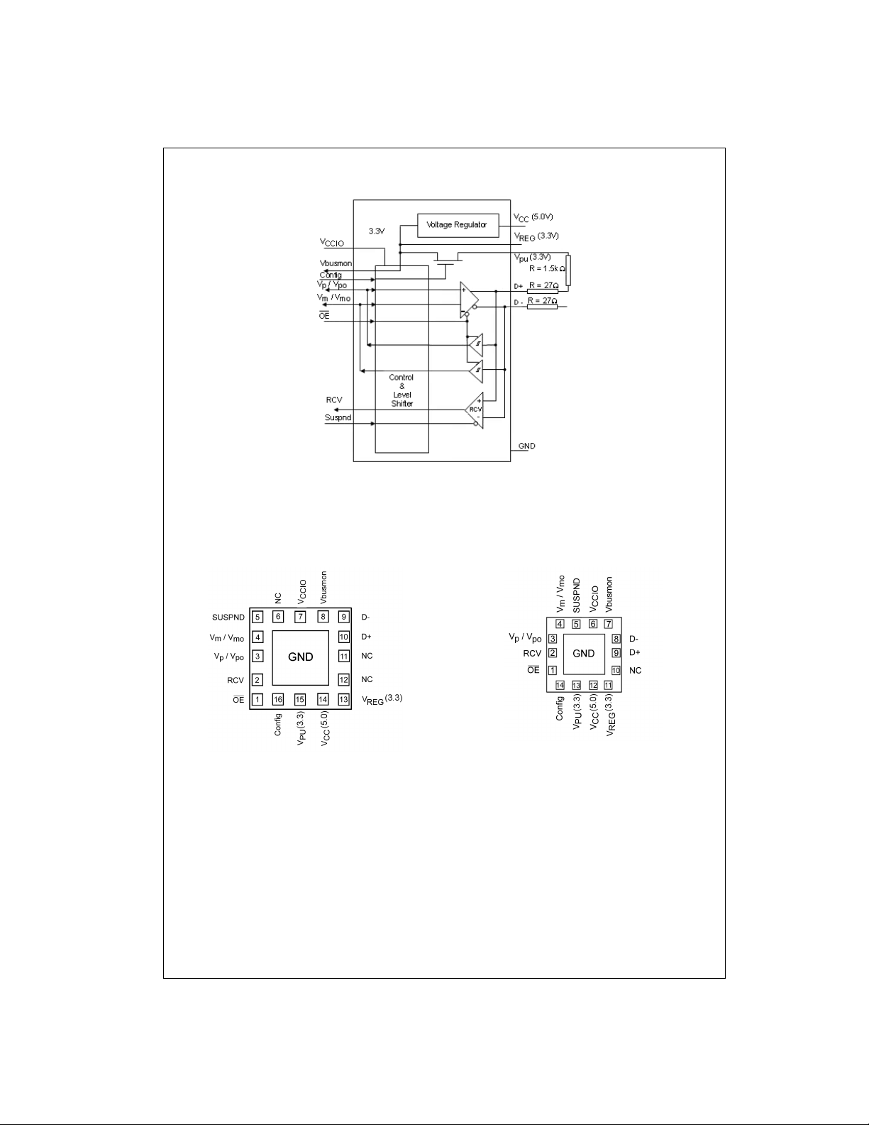
Logic Diagram
USB1T1103
Connection Diagrams
MLP16 GND Exposed Diepad
(Bottom View)
MLP14 GND Exposed Diepad
(Bottom View)
www.fairchildsemi.com 2
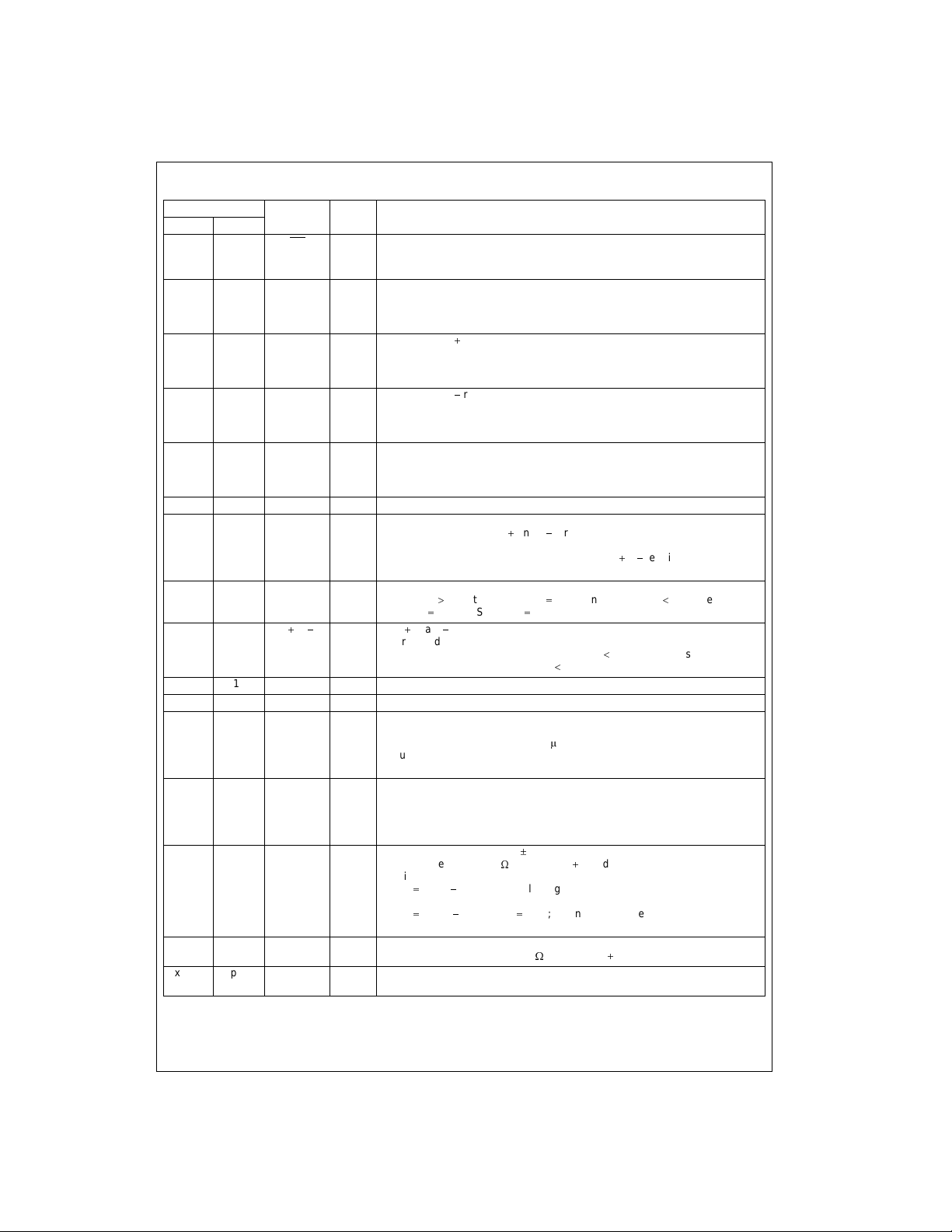
Terminal Descriptions
Te rminal Number
MLP14 MLP16
11 OE
2 2 RCV O Receive Data Output:
33V
44V
5 5 SUSPND I Suspend:
— 6 NC No Connect
67V
7 8 Vbusmon O Vbus monitor output (CMOS level relative to V
9, 8 10, 9 D
10 11 NC No Connect
— 12 NC No Connect
11 13 V
12 14 V
13 15 V
14 16 Config I USB connect or disconnect software control input.
Exposed
Diepad
Exposed
Diepad
Terminal
Name
I/O Terminal Description
I Output Enable:
Active LOW enables the transceiver to transmit data on the bus. When not
active the transceiver is in the receive mode (CMOS level is relative to V
Non-inverted CMOS level output for USB differential Input (CMOS output level
). Driven LOW when SUSPN is HIGH; RCV output is stable
CCIO
po
mo
p/Vpo
m/Vmo
is relative to V
and preserved during SE0 condition.
I/O Single-ended D receiver output VP (CMOS level relative to V
Used for external detection of SE0, error conditions, speed of connected device;
Terminal also acts as drive data input V
Output drive is 4 mA buffer.
I/O Single-ended D receiver output Vm (CMOS level relative to V
Used for external detection of SE0, error conditions, speed of connected device;
Terminal also acts as drive data input V
Output drive is 4 mA buffer.
Enables a low power state (CMOS level is relative to V
SUSPND terminal is active (HIGH) it will drive the RCV terminal to logic “0”
state.
CCIO
, D
(3.3V) Internal Regulator Option:
REG
Supply Voltage for digital I/O terminals (1.65V to 3.6V):
When not connected the D
is totally independent of V
(3.3) voltage. For V
V
REG
Impedance and the V
!
When Vbus
Vbusmon
4.1V then Vbusmon HIGH and when Vbus 3.6V then
LOW. If SUSPND HIGH then Vbusmon is pulled HIGH.
and D terminals are in 3-STATE. This supply bus
(5V) and V
CC
disconnected the O/O terminals are HIGH
CCIO
(3.3V) is turned off.
PU
REG
AI/O Data , Data :
Differential data bus conforming to the USB standard. Terminals are HIGH
Impedance for bus powered mode when Vbus
HIGH Impedance when V
Regulated supply output voltage (3.0V to 3.6V) during 5V operation;
decoupling capacitor of at least 0.1
/ Vbus V
REG
REG
P
F is required.
Regulator ByPass Option:
Used as supply voltage input for 3.3V operation.
(5.0V) Internal Regulator Option:
CC
(3.3V) Pull-up Supply Voltage (3.3 V r 10%):
PU
Used as supply voltage input (4.0V to 5.5V); can be connected directly to USB
line Vbus.
Regulator ByPass Option:
Connected to V
Connect an external 1.5k
REG
(3.3V)
:
resistor on D (FS data rate);
Terminal function is controlled by Config input terminal:
LOW VPU (3.3V) is floating (HIGH Impedance) for zero pull-up cur-
Config
rent.
Config
HIGH VPU (3.3V) 3.3V; internally connected to V
is OFF in disable mode.
V
PU
:
Configures 3.3V to external 1.5k
resistor on D when HIGH.
GND GND GND supply down bonded to exposed diepad to be connected to the PCB GND.
):
CCIO
(see Table 1 and Table 2).
):
CCIO
(see Table 1 and Table 2).
). While the
CCIO
(3.3V), and must never exceed the
):
CCIO
3.6V. For ByPass Mode then
minimum.
(3.3V).
REG
CCIO
USB1T1103
)
3 www.fairchildsemi.com
Functional Description
The USB1T1103 transceiver is designed to convert CMOS
data into USB differential bus signal levels and to convert
USB differential bus signal to CMOS data.
To minimize EMI and noise the outputs are edge rate con-
USB1T1103
trolled with the rise and fall times controlled and defined for
full speed data rates on ly (12Mbits/s). The rise, fall tim es
are balanced between the differential terminals to minimize
skew.
The USB1T1103 differs from earlier USB Transceiver in
that the V
and Vpo/Vmo terminals are now I/O terminals
p/Vm
Functional Tables
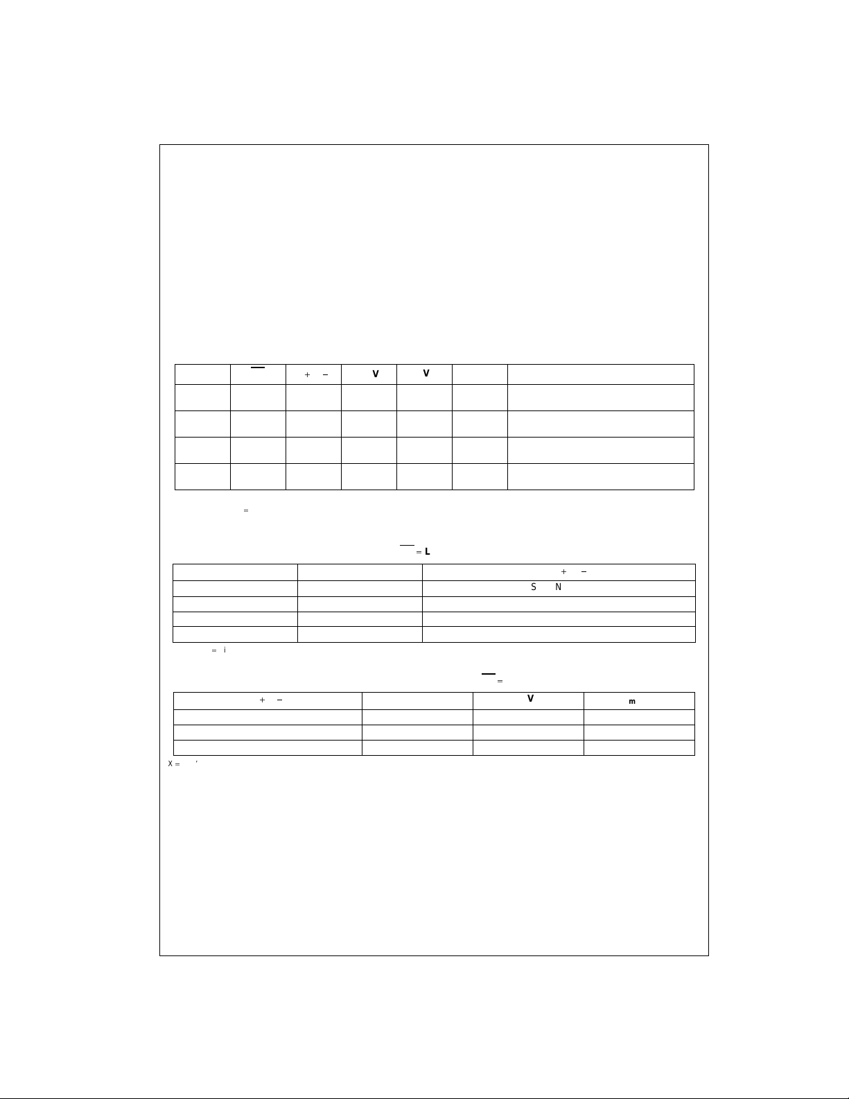
TABLE 1. Function Select
SUSPND OE D, D
L L Driving &
L H Receiving
H L Driving Inactive
H H 3-STATE
Note 1: Signal levels is functio n of connection and/or pull-up/pull-down re s is to rs .
Note 2: For SUSPND
the single-ended rec eivers of the V
HIGH mode the differential receiver is inactive and the output RCV is forced LOW. The out-of-suspend signaling (K) is detected via
TABLE 2. Driver Function (OE L) using Differential Input Interface
V
m/Vmo
L L SE0 (Note 3)
L H Differential Logic 1
H L Differential Logic 0
H H Illegal State
Note 3: SE0 Single Ended Zero
Receiving
(Note 1)
(Note 1)
and Vm/Vmo terminals.
p/Vpo
RCV
Active V
Active V
(Note 2)
Inactive
(Note 2)
Vp/V
po
rather than discrete input and output terminals. Table 1
describes the specific terminal functionality selection. T able
2 and Table 3 describe the specifi c Truth Tables for Driver
and Receiver operating functions.
The USB1T1103 also has the capab ility of various power
supply configurations, including a disable mode for V
disconnected, to support mixed voltage supply applications
(see Table 4) and Section 2.1 for detailed descriptions.
V
p/Vpo
Input Vmo Input Normal Driving
po
Output Vm Output Receiving
p
V
Input Vmo Input Driving during Suspend
po
Output Vm Output Low Power State
V
p
Vm/V
mo
(Differential Receiver Active)
(Differential Receiver Inactive)
Function
Data (D / D)
CCIO
TABLE 3. Receiver Function (OE H)
, D
D
RCV
V
p/Vpo
Differential Logic 1 H H L
Differential Logic 0 L L H
SE0 X L L
X Don’t Care
RCV(0) denotes th e signal level on output R C V jus t prior to the SE0 or SE1 ev ent. This level is stable during the SE0 or SE1 eve nt period.
www.fairchildsemi.com 4
Vm/V
mo
Power Supply Configurations and Options
The three modes of power supply operation are:
• Normal Mode: Regulated Output and Regulator Bypass
1. Re gula ted Ou tpu t: V
is connected and VCC(5.0)
CCIO
is connected to 5V (4.0 V to 5.5V) and the internal
voltage regulator then produces 3.3V for the USB
connections.
2. Internal Regulator Bypass Mode: V
nected and both V
(5.0) and V
CC
CCIO
(3.3) are con-
REG
is con-
nected to a 3.3V source (3.0V to 3.6V).
In both cases for n orm al mo de the V
is an indepen-
CCIO
dent voltage source (1 .65V to 3 .6V) that i s a functi on of
the external circuit configuration.
• Sharing Mode: V
V
are not connected. In this mode the D and D ter-
REG
is only supply connected. VCC and
CCIO
minals are 3-STATE and the USB1T1103 allows external
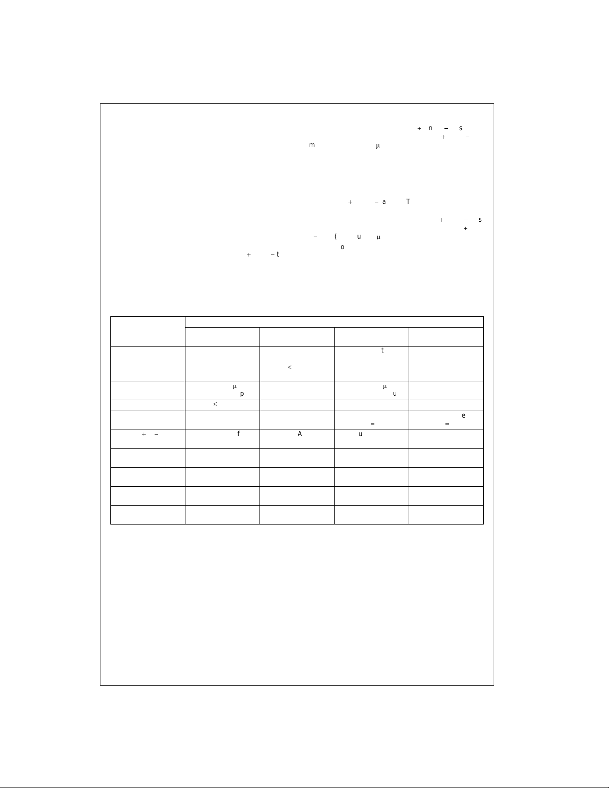
TABLE 4. Power Supply Configuration Options
Power Supply Mode Configuration
Terminals
(5V) Connected to 5V
V
CC
(3.3V) 3.3V, 300PA
V
REG
V
CCIO
V
(3.3V) 3-STATE (off) 3-STATE (Off) 3.3V Available if
PU
, D
D
, Vm/V
V
p/Vpo
mo
Disable Sharing
Not Connected
source
Not Connected 3.3V, 300 PA
Regulated Output
d
0.5V 1.65V to 3.6V Source 1.65V to 3.6V Source 1.65V to 3.6V Source
3-STATE (off) 3-STATE Function of
Invalid [I] L Function of
RCV Invalid [I] L Function of
Vbusmon Invalid [I] L Function of
OE, SUSPND, Config Hi-Z Hi-Z Function of
Invalid [I] I/O are to be 3-STATE, outputs to be LOW.
signals up to 3.6V to s hare the D
Internally the circuitry limits leakage from D
minals (maximum 10
in low power (suspended) state. Terminals Vbusmon
and RCV are force d LOW as a n indica tion of th is mode
with Vbusmon being ignored during this state.
• Disable Mode: V
nected, or V
this mode D
CCIO
and V
CC
and D are 3-STATE and VPU is HIGH
Impedance (switch is turned off). The USB1T1103 allows
external signals up to 3.6V to sha re the D
lines. Internally the circuitry limits leakage from D
D
pins (maximum 10PA).
A summary of the Suppl y Configurations is described in
Table 4.
Normal (Regulated
Output)
Connected to 5V
or
3.6V
Source
Regulated Output
Config
Mode Set Up
Mode Set Up
Mode Set Up
Mode Set Up
Mode Set Up
and D bus lines.
P
A) and V
CCIO
and D ter-
such that device is
is not connected. VCC is con-
are connected. 0V to 3.3V in
REG
and D bus
Normal (Regulator
Bypass)
Connected to V
(3.3V)
[Max Drop of 0.3V]
(2.7V to 3.6V)
Connected to 3.3V
Source
3.3V Available if
HIGH
Config HIGH
Function of
Mode Set Up
Function of
Mode Set Up
Function of
Mode Set Up
Function of
Mode Set Up
Function of
Mode Set Up
REG
USB1T1103
and
5 www.fairchildsemi.com
 Loading...