Fairchild USB1101 service manual

查询USB1101供应商
June 2005
Revised June 2005
USB1101
USB 2.0 FS Peripheral Transceiver (Preliminary)
General Description
The USB1101 provides a USB FS Transceiver functionality
with voltage level translation that is compliant to USB Specification Rev 2.0. The device allows interfacing of USB
Application specific devices with supply voltages ranging
from 1.65V to 3.6V with the physical layer of Universal
Serial Bus. It is capable of operating at 12Mbits/s (full
speed) data rates and hence is fully compliant to USB
Specification Rev 2.0. It supports the DAT_VP/SE0_VM
interface on the host side but offers reduced pin cou nt and
package size. The USB1101 has host side supply rail for
1.65V to 3.6V.
Features
■ Complies with USB Specification Rev 2.0
■ Supports DAT_VP/SE0_VM host mode
■ Utilizes digital inputs and outputs to transmit and receive
USB cable data
■ Supports full speed (12Mbits/s) data rates
■ Ideal for portable electronic devices
■ MicroPak
■ Host side V
¥
1.6mm x 2.1mm
technology package ( 10 pin)
CCIO
1.65V to 3.6V
Applications
•PDA
• PC Peripherals
• Cellular Phones
•MP3 Players
• Digital Cameras
• Information Appliance
Preliminary
USB1101 USB 2.0 FS Peripheral Transceiver (Preliminary)
Ordering Code:
Order Package Package
Number Number Top Mark
USB1101L10X MAC010A UB 10-Lead MicroPak, 1.6 mm x 2.1mm 5k Units on Tape and Reel
Package Description Supplied As
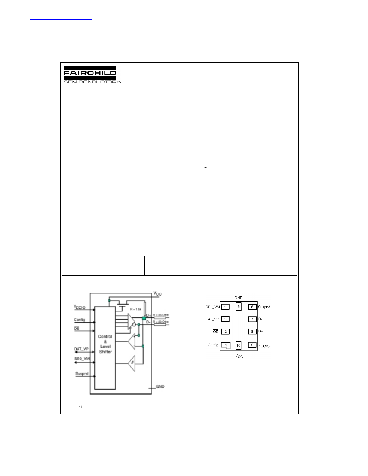
Connection Diagram
(Bottom View)
MicroPak¥ is a trademark of Fair ch ild Semiconductor Co rporation.
© 2005 Fairchild Semiconductor Corporation DS500923 www.fairchildsemi.com

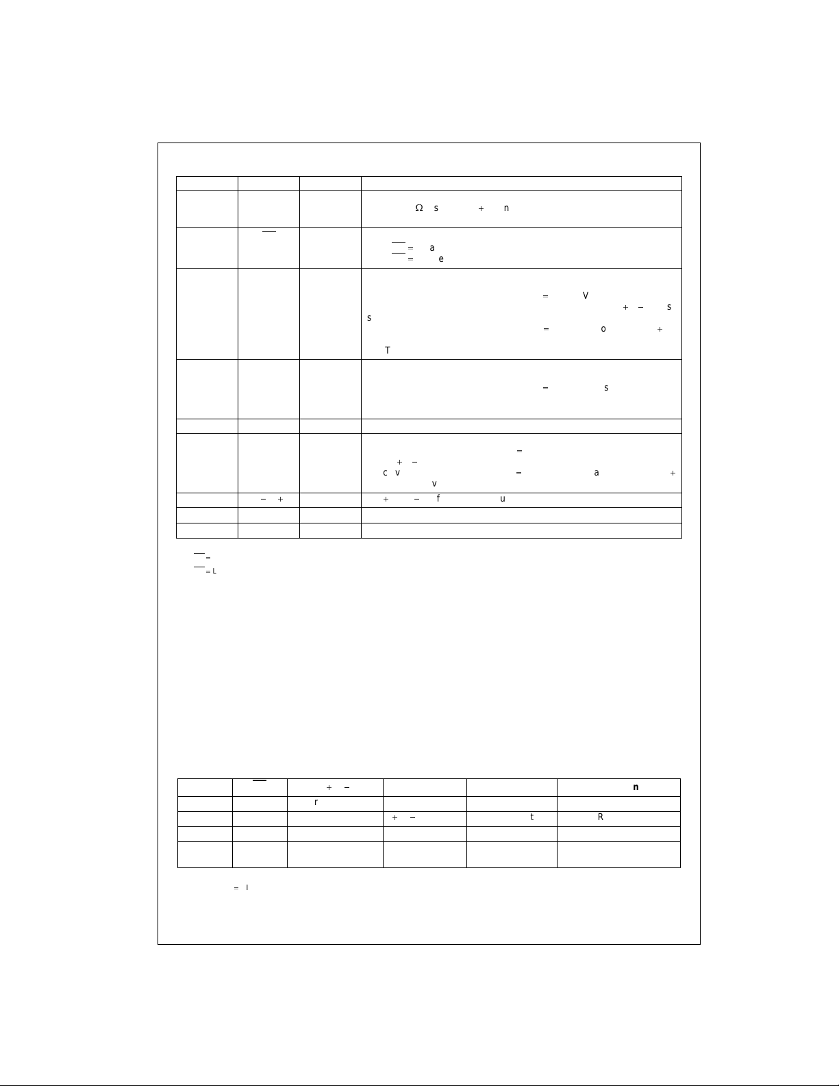
Pin Description
Pin Number Pin Name I/O Pin Description
USB1101
1 Config I USB connect or disconnect software control input. Configures 3.3V to
:
internal 1.5k
port then this pin is hard-wired to GND.
2OE
I Output Enable (active LOW)
When OE
When OE
3 DAT_VP I/O When in transmit mode
(CMOS level relative to V
When in receive mode
data output comprised of the differential input data from the D
(see Table 2);
When in receive mode
data.
(see Table 1 and Table 2) Output drive is 2mA (min) buffer
4 SE0_VM I/O When in transmit mode
tive to V
When in receive mode
resistor on D when HIGH. If device is used as Downstream
L transmit mode is enabled
H receive mode (CMOS level is relative to V
(Note 2)
CCIO
(Note 1)
(Note 1)
(Note 2)
).
CCIO
(Note 1)
put (see Table 2)
(see Table 1 and Table 2). Output drive is 4ma (min) buffer
5 GND GND GND
6 Suspnd I Enables a low power state (CMOS level is relative to V
In receive mode
of the D
In receive mode
/D
lines.
(Note 1)
with Suspnd L the DAT_VP pin will be a function
(Note 1)
with Suspnd H DAT_VP will have the value of D
such that the device can still monitor out-of-suspend signaling.
, D
7, 8 D
9V
10 V
CCIO
CC
AI/O Data, Data. Differential data bus conforming to the USB standard
Pwr Supply Voltage for host side digital I/O pins (1.65V to 3.6V)
Pwr Supply Voltage Input (3.0V to 3.6V)
Preliminary
) is enabled.
DAT_VP is a single-ended host data input
).
and Suspnd L DAT_VP is a single ended
with Suspnd H DAT_VP outputs the D
SE0_VM is a data input (CMOS level rela-
and Suspnd L, SE0_VM is used as an out-
CCIO
CCIO
/D
inputs
).
Note 1: OE H
Note 2: OE
L
Functional Description
The USB1101 transceiver is designed as an Upstream facing port device to convert CMOS d ata into US B differen tial
bus signal levels and to co nve rt USB differe ntial b us si gn al
to CMOS data. If you wish to use these as downstream
devices, Config must be hard-wired to GND.
To minimize EMI and noise the outputs are edge rate controlled with the rise and fall times controlled and defined for
full speed data rates only (12Mbits/s). The rise and fall
times are balanced between the differential pins to minimize skew.
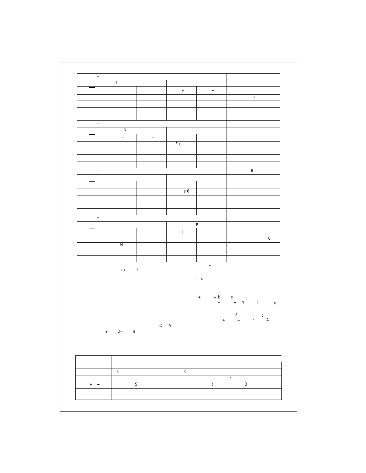
TABLE 1. Function Select
Suspnd OE D, D
L L Transmitting Host Data Input SE0_VM Host Input Normal Driving
L H Receiving (Note 3) D
H L Transmitting (Note 4) Host Data Input SE0_VM Host Input Driving while Suspended
H H Driver is 3-STATE
DAT_VP Output SE0_VM Output Suspended
(Note 4)
Note 3: Signal levels is functio n of c onnection, Config and/or pull-up/pull-down resistors.
Note 4: For Suspnd
HIGH mode the differential receiver is inactive.
The USB1101 supports the DAT_VP/SE0_VM format from
the OTG Transceiver Specification using the DAT_SE0
Mode. Table 1 describes the specific pin functionality selection and Table 2 describes the specific Truth Tables for
Driver, Receiver, and Suspended operating functions.
The USB1101 has the capability of serving Self Powered
power supply configu rations only but interfaces to mixed
voltage supply applications.
DAT_VP SE0_VM Function
, D Diff Output SE0_VM Output Receiving
(Internal Low Power Mode)
www.fairchildsemi.com 2

Preliminary
TABLE 2. Driver, Receiver, and Suspend Function Select
Suspnd
L Transmit Mode
Inputs Outputs
OE
DAT_VP SEO_VM D
L L L L H Differential Logic 0
L H L H L Differential Logic 1
L L H L L SE0
L H H L L SE0
Suspnd
L Receive Mode
Inputs Outputs
OE
D
D
H L L DIFF (Note 5) H
HHLHL
HLHLL
H H H DIFF (Note 5) L
Suspnd
L Receive Mode While Suspended
Inputs Outputs
OE
D
D
H L L L (Note 6) H
H H L H (Note 6) L
H L H L (Note 6) L
H H H H (Note 6) L
Suspnd
H Transmit Mode
Inputs Outputs
OE
DAT_VP SEO_VM D
L L L L H Differential Logic 0
L H L H L Differential Logic 1
L L H L L SE0
L H H L L SE0
Note 5: DIFF denotes that t he output of the differential receiver is out put via DAT_VP when Sus pnd L. This output sh ould also not be ga te d by the SE0 or
SE1 condition when a s kew betw een D
mation.
Note 6: This is the internal single en ded output that is outp ut on to DAT_VP when Suspnd
and D signals could resu lt in the s hort SE0 or S E1 cond ition s. Plea se ref er to Expe ctatio n Note s for further infor-
D
DAT_VP SEO_VM
DAT_VP SEO_VM
D
H and in receive mode.
USB1101
Power Supply Configurations and Options
The modes of power supply operation include:
1. Self Powered Mode: V
is connected to 3.3V source
CC
(3.0V to 3.6V). This external supply connection provides the 3.3V for the USB pull-up sour ce, the receiv er
input and driver output circuitry.
2. Sharing Mode: V
In this mode the D
is connected and VCC is d 0.8V.
CCIO
and D pins are 3-STATE and the
USB1101 allows external signals up to 3.6V to share
TABLE 3. Power Supply Configuration Options
Pin
V
CC
V
CCIO
, D
D
DAT_VP,
Sharing Self Powered Disable
d
0.8V or Not Connected Connected to 3.3V Source Connected to 3.3V Source
1.65V to 3.6V Source 1.65V to 3.6V Source
3-STATE Function of Mode Set Up 3-STATE
H Function of Mode Set Up (Invalid)
SE0_VM
Power Supply Mode Configuration
the D
leakage from D
V
CCIO
3. Disable Mode: V
In this mode the D
device is in low power state.
A summary of the Supply Configuration is described in
Table 3.
3 www.fairchildsemi.com
and D bus lines. Internally the circuitry limits
and D pins (maximum 10PA) and
such that the device is in low power state.
is d 0.5V and VCC is connected.
CCIO
and D pins are 3-STATE and the
d
0.5V or Not Connected
 Loading...