


www.fairchildsemi.com
AN-9066
UniFET™ — Optimized Switch for Discontinuous Current
Mode Power Factor Correction
Abstract
This application note discusses merits of planar technology
power MOSFET in discontinuous current mode power
factor correction application. In most test conditions it is
cost competitive and gives performance benefits compared
to a super-junction technology device. The benefits are
verified through the mathematical simulation and systemlevel experiments. A new planar technology power
MOSFET from Fairchild shows faster switching
characteristics that contribute to higher efficiency and lower
device temperature.
Introduction
Switch-mode power supplies are increasingly being
designed with an active power factor correction at the input
stage to meet international regulations for harmonics. The
boost topology in discontinuous current mode (DCM) is
most suitable power factor correction (PFC) method for
converters with less than 300W power rating[1]. In this
topology, the switching-on power loss of boost switch is
negligible, and the major power losses are the switching-off
losses and conduction losses. After the super-junction
devices have been introduced, they are often considered as
optimized switches for active power factor correction
because of extremely low on-resistance and highly nonlinear capacitance curves. In the discontinuous current mode
power factor correction, however, the conventional planar
devices can compete against the powerful super-junction
family. This article shows that Fairchild’s UniFET™ power
MOSFET can provide performance superior to the superjunction devices in the discontinuous current mode power
factor correction applications.
Power MOSFET Technologies
The super-junction technology utilizes deep P-type pillar
structure in the body of the power MOSFET. The effect of
the pillars is to confine the electric field in the lightly doped
epitaxial region of the power MOSFET. Thanks to this Ppillar, the resistivity of N-epi can be reduced compared to
the conventional planar technology, while maintaining the
same breakdown voltage. Therefore, typical on-resistance of
the super-junction MOSFETs is only one third of the
conventional planar power MOSFETs at the same chip size.
Most commercially available super-junction devices adopt
multiple epi-layers to build the deep P-pillar structure. The
multi-epi process, however, has some disadvantages, such
© 2009 Fairchild Semiconductor Corporation www.fairchildsemi.com
Rev. 1.0.1 • 4/3/09
as increased process steps and higher manufacturing cost. In
contrast, the UniFET™ power MOSFET utilizes a planar
double-diffused metal-oxide semiconductor (DMOS)
process that is very mature and highly cost competitive.
Moreover, it has improved ring terminations and optimized
active cell structures compared to the conventional planar
power MOSFETs. The resulting specific on-resistance of
the UniFET is even close to some super-junction devices at
500V of breakdown voltage range.
The planar power MOSFETs also have higher reliability
than the super-junction MOSFETs under unclamped
inductive switching (UIS) condition, which can occur
during power supply power-up or AC line transient. The
devices can enter breakdown, and even be destroyed, in the
worst situations. Typically, the planar MOSFETs are much
better than the super-junction devices in UIS mode. The
newest super-junction technology enabled equivalent UIS
rating to the planar MOSFETs at unit area; however, its
practical rating as a single device is still inferior to planar
MOSFETs because of smaller die size. The UIS ruggedness
of UniFET is also far better than previous generations of
planar technology. For an example, a 265mΩ, 500V
UniFET shows more than 80A of avalanche current under
low coil UIS test. Moreover, it does not fail at all in the test.
On the contrary, a conventional planar MOSFET with same
on-resistance failed at around 40A. The improved
ruggedness ensures enhanced reliability. In terms of
switching performance, a gate charge is one of the
benchmarks to compare different devices. The UniFET has
a smaller gate charge, faster switching characteristics, and
reduced switching power losses than the conventional
planar MOSFETs. Some typical electric characteristics
benchmarks are shown in
Table 1. Gate Charge and Parasitic Capacitance
Benchmark Data
Q
FDB12N50 22nC 140pF 985Pf 12pF
FQB12N50 39nC 220pF 1550pF 25pF
FDA16N50 32nC 235pF 1495pF 20pF
FQA16N50 60nC 325pF 2300pF 35pF
Note:
1. FDB12N50 and FDA16N50 are UniFET™. FQB12N50
and FQA16N50 are QFET
planar power MOSFET.
Table 1.
G
C
OSS
®
, is a previous generation of
C
ISS
C
RSS
AN-9066 APPLICATION NOTE
Discontinuous Current Mode Power
Factor Correction
Generally, power factor correction circuits have used a
boost topology because it is simple and low costs. There are
two modes of the power factor correction boost circuit
operation. One is continuous current mode (CCM) that has
continuous inductor current. This mode has many benefits,
like lower core loss and ripple current and a smaller input
filter; but it requires very fast reverse recovery diode as the
boost diode since the boost switch in being switched on
while the inductor current is not zero. The discontinuous
current mode switches on the boost switch when the
inductor current is zero, allowing less expensive diodes to
be used. The turn-on loss of the boost switch is also
negligible. Usually, the discontinuous current mode is used
for small power supplies, 300W or less, that have relatively
small inductor current, but are very sensitive to cost
constraints.
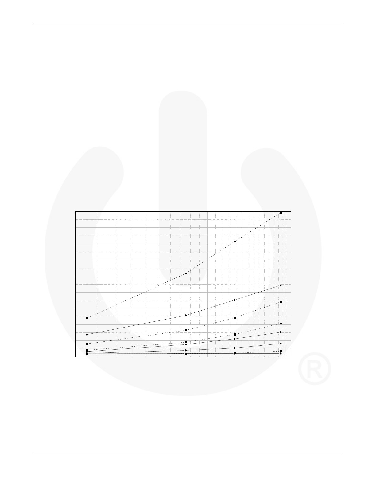
450
Simulation and Experimental
Results
Conduction loss is easy to evaluate because the R
is clearly stated in datasheets, but the switching loss varies
greatly by the circuit conditions. To compare the switching
performance in the system, one UniFET and one superjunction device are selected and evaluated. An inductive
switching test board was used to measure switching loss at
turn-off transient. In this way, it is possible to keep the
important test variables, like drain current and external
series gate resistor, under control.
Figure 1 shows the energy loss curves with different
conditions of the series gate resistor and the drain-current.
The solid traces indicate the losses of the UniFET and the
dotted traces are losses of the super-junction device. There
are four different lines per device, according to the pre-set
drain current levels. The drain current levels are 20A, 10A,
6.5A, and 1.8A from top to bottom.
DS(on)
value
400
350
300
250
200
150
100
S wit c hin g- o ffE n er g yLos s [ µJ ]
50
0
4 8 12 16 20 24
External Series Gate Resistance [Ω]
© 2009 Fairchild Semiconductor Corporation www.fairchildsemi.com
Rev. 1.0.1 • 4/3/09 2
450
400
350
300
250
200
150
100
Switching-Off Enery Loss [µJ]
50
0
4 8 12 16 20 24
External Series Gate Resistance[Ω]
Figure 1. Energy Losses During Switching-Off Transition
www.fairchildsemi.com
© 2009 Fairchild Semiconductor Corporation www.fairchildsemi.com
Rev. 1.0.1 • 4/3/09
AN-9066 APPLICATION NOTE
It is obvious that the UniFET has far less energy loss than
the super-junction device at high current condition. Also,
the UniFET outperforms the super-junction device as gate
resistance becomes larger. The only test point where the
super-junction device does better than the UniFET is at the
lowest current and the smallest gate resistor. The power loss
during switching-on transition has not been evaluated
because it is negligible in the DCM PFC. Based on the
switching performance evaluation results, a simulation was
preformed to analyze system-wide performance. A 200Wrated DCM PFC was assumed for the simulation and
simulation time has set to a single cycle of AC input.
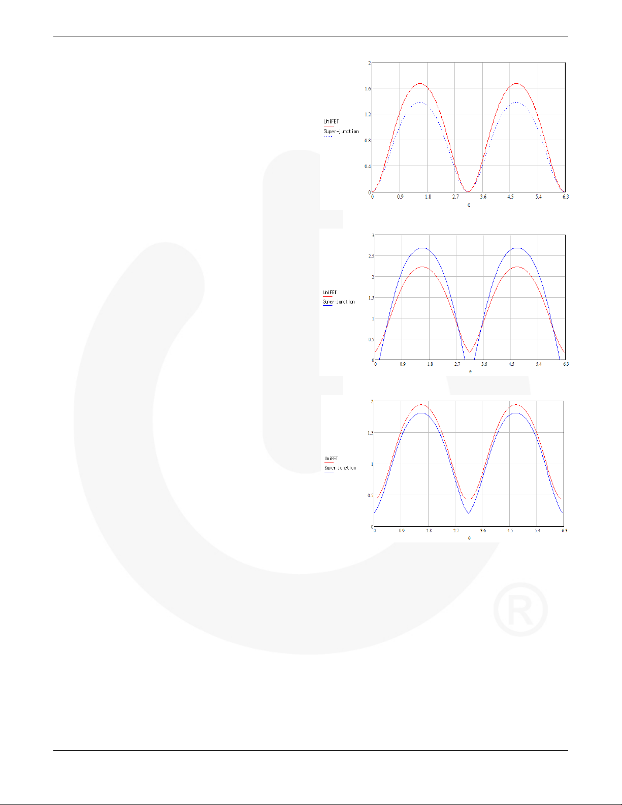
The simulated conduction losses are shown in
lower R
low R
junction devices.
makes the less conduction loss. Clearly, the
DS(on)
is the most significant benefit of the super-
DS(on)
Figure 3 shows combined loss curves at
external series gate resistance of 15Ω. In
Figure 2. The
Figure 3, the
estimated performance of the UniFET is better than the
super-junction device due to its fast switching
characteristics. The distortion at zero-crossing current
regions is due to convergence error of the simulation. With
more switching energy loss data, the convergence error can
be reduced.
When lowered to 4.4Ω gate resistor, the super-junction
device is slightly better than the UniFET in
shown in
Figure 1, there are not much difference in
Figure 4. As
switching-off power losses with small resistor and low drain
current conditions.
To verify simulation results, both devices are evaluated
using a state-of-the-art game console power supply. The
devices are applied to DCM PFC block of the power supply
and the test conditions are set as V
P
OUT
=225W, R
=22Ω, and R
G(on)
G(off)
=3.3Ω.
=110VAC/60Hz,
IN
Figure 2. Simulated Conduction Losses In Watt
Figure 3. Simulated Combined Losses with RG=15Ω
Figure 4. Simulated Combined Losses with RG=4.4Ω
© 2009 Fairchild Semiconductor Corporation www.fairchildsemi.com
Rev. 1.0.1 • 4/3/09 4
AN-9066 APPLICATION NOTE
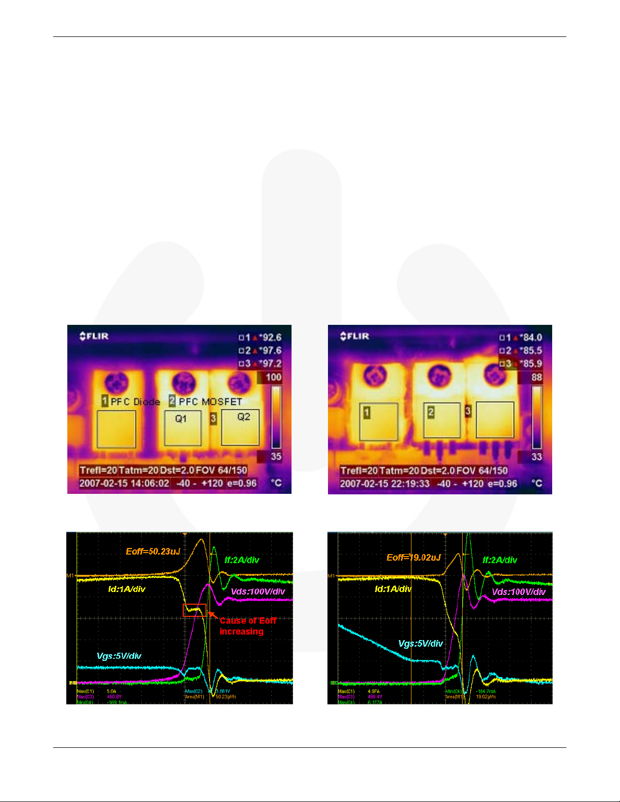
Figure 5, an IR camera was used to measure device
In
temperature. Three measurement points are a PFC diode and
two paralleled PFC MOSFETs. Even with small gate
resistor, the UniFET temperature is lower than the superjunction device by around 10 degrees. The reason for this
lower temperature is smaller switching losses, as shown in
Figure 6. The UniFET switching-off energy loss at the peak
of AC input voltage is less than a half of the super-junction
device switching loss. There is a little plateau in the drain
current of the super-junction that makes switching-off loss
bigger. There was no such waveform in the bench test.
Perhaps it is due to different gate drive circuitry and printed
circuit board layout.
Recently, dedicated controllers for the interleaved
discontinuous current mode power factor correction were
introduced to the market. The interleaved CRM PFC
technique is a good alternative solution to implement highdensity, cost-effective converters with an extended input
power range. It quickly became mainstream topology in
switching power supplies for flat panel displays because the
interleaving technique can reduce the total system cost
compared to CCM topology. Although it requires a pair of
boost inductors, boost switches, and rectifiers, it can use
small-sized filters, smaller high-voltage aluminum
electrolytic capacitor, a less-expensive 500V-rated boost
switches, and slower rectifiers. In addition, making the flat
panel TV slim is a trend and the smaller components are a
crucial requirement for a low-profile switching power
supply.
As the interleaving PFC is also operated in discontinuous
current mode, the UniFET can be quite competitive with the
super-junction device. To compare system performance, the
UniFET and the super-junction device were tested with an
interleaved DCM PFC evaluation board. The evaluation was
done using an interleaved CRM controller with phase
management. Two RURP860 ultrafast rectifiers are applied
as boost diodes. The test conditions are set as
=115VAC/60Hz,R
V
IN
=10Ω, R
G(on)
=3.9Ω, room
G(off)
temperature without fan, and an external bias for controller
supply voltage.
(a) Super-Junction Device (b) UniFET
Figure 5. Device Temperature (Not Same Scale)
™
(a) Super-Junction Device (b) UniFET
Figure 6. Switching-Off Energy Loss
© 2009 Fairchild Semiconductor Corporation www.fairchildsemi.com
Rev. 1.0.1 • 4/3/09 5
™
AN-9066 APPLICATION NOTE
98
97
96
95
Efficiency [%]
94
93
0 100 200 300 400 500 600
Output Power [W]
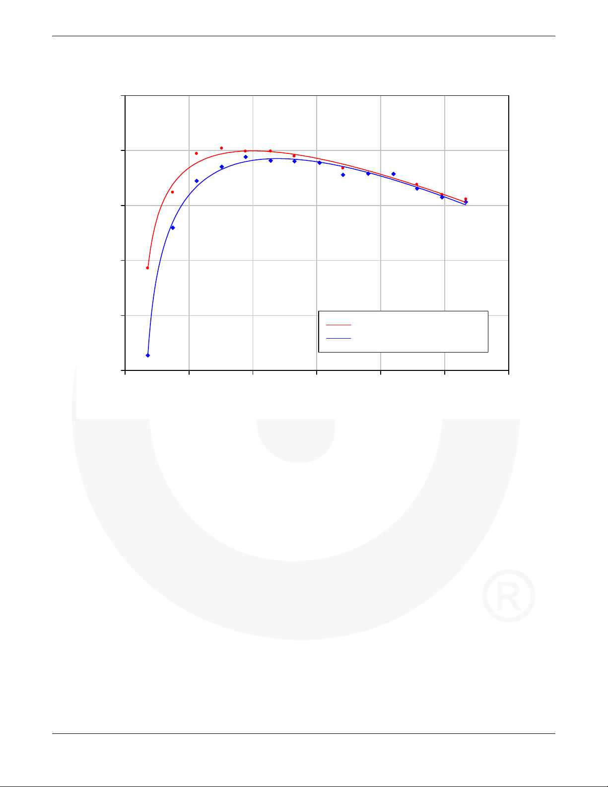
Figure 7. Efficiency Curves with 115V AC Input
The efficiency results are shown in
much difference in efficiency when in heavy load.
Basically, the super-junction device has lower R
the UniFET at same drain current rating and therefore will
have more conduction loss advantage as the load becomes
heavier. The smaller switching loss of the UniFET
compensates its higher R
DS(on)
the UniFET shows slightly better performance. In the lightload area, the switching loss dominates the power losses
and the UniFET surpasses the super-junction device.
Figure 7. There is not
than
DS(on)
well in heavy load area and
UniFET, 20A/500V
Super-juncti on, 21A/500V
Conclusion
The performance of the UniFET™ was evaluated at both
device level and system level. It showed good results
against the super-junction device and can be an optimum
solution in DCM PFC application as long as required
breakdown voltage of the boost switch is 500V. The
interleaved DCM PFC is gaining attention recently and this
is another application where the UniFET can be considered
as a high-performance, cost-effective boost switch.
© 2009 Fairchild Semiconductor Corporation www.fairchildsemi.com
Rev. 1.0.1 • 4/3/09 6

AN-9066 APPLICATION NOTE
Table 2. 500V UniFET™ Line-up
Part Number BV
DSS
R
DS(ON)
Max (W)
at VGS = 10V
Qg Typ. (nC)
at VGS = 5V
ID (A)
QRR Typ. (nC)
at diF/dt=100A/µs
Package
FDD5N50U 500 2.000 11.0 3.00 33 TO-252(DPAK)
FDD5N50F 500 1.550 11.0 3.50 120 TO-252(DPAK)
FDD5N50 500 1.400 11.0 4.00 1800 TO-252(DPAK)
FDPF5N50FT 500 1.550 11.0 4.50 120 TO-220F
FDP5N50 500 1.400 11.0 5.00 1800 TO-220
FDPF5N50T 500 1.400 11.0 5.00 1800 TO-220F
FDD6N50F 500 1.150 15.0 5.50 150 TO-252(DPAK)
FDU6N50 500 0.900 12.8 6.00 1700 TO-251(IPAK)
FDD6N50 500 0.900 12.8 6.00 1700 TO-252(DPAK)
FDPF7N50F 500 1.150 15.0 6.00 150 TO-220F
FDP7N50 500 0.900 12.8 7.00 1700 TO-220
FDPF7N50 500 0.900 12.8 7.00 1700 TO-220F
FDB12N50U 500 0.800 21.0 10.00 100 TO-263(D2PAK)
FDB12N50F 500 0.700 21.0 11.50 370 TO-263(D2PAK)
FDPF12N50FT 500 0.700 21.0 11.50 370 TO-220F
FDB12N50 500 0.650 22.0 11.50 3500 TO-263(D2PAK)
FDP12N50 500 0.650 22.0 11.50 3500 TO-220
FDPF12N50T 500 0.650 22.0 11.50 3500 TO-220F
FDPF13N50FT 500 0.540 30.0 12.00 450 TO-220F
FDB15N50 500 0.380 33.0 15.00 5000 TO-263(D2PAK)
FDP15N50 500 0.380 33.0 15.00 5000 TO-220
FDH15N50 500 0.380 33.0 15.00 5000 TO-247
FDP16N50 500 0.390 32.0 16.00 5000 TO-220
FDPF16N50T 500 0.380 32.0 16.00 5000 TO-220F
FDA16N50 500 0.380 32.0 16.50 5000 TO-3P
FDP18N50 500 0.265 45.0 18.00 5400 TO-220
FDPF18N50 500 0.265 45.0 18.00 5400 TO-220F
FDPF18N50T 500 0.265 45.0 18.00 5400 TO-220F
FDA18N50 500 0.265 45.0 19.00 5400 TO-3P
FDP20N50F 500 0.260 50.0 20.00 500 TO-220
FDPF20N50FT 500 0.260 50.0 20.00 500 TO-220F
FDA20N50F 500 0.260 50.0 22.00 500 TO-3P
FDP20N50 500 0.230 45.6 20.00 7200 TO-220
FDPF20N50T 500 0.230 45.6 20.00 7200 TO-220F
FDA20N50 500 0.230 45.6 22.00 7200 TO-3P
FDA24N50 500 0.190 65.0 24.00 8100 TO-3PN
FDA24N50F 500 0.200 65.0 24.00 1400 TO-3PN
FDA28N50 500 0.155 80.0 28.00 8000 TO-3PN
FDA28N50F 500 0.175 80.0 28.00 1380 TO-3PN
FDH44N50 500 0.120 90.0 44.00 14000 TO-247
FDH45N50F 500 0.120 105.0 45.00 640 TO-247
FDA50N50 500 0.105 105.0 48.00 10000 TO-3P
© 2009 Fairchild Semiconductor Corporation www.fairchildsemi.com
Rev. 1.0.1 • 4/3/09 7

AN-9066 APPLICATION NOTE
Reference
[1] Fairchild application note, AN-42047 Power Factor Correction Basics
Author
Won-suk Choi and Sung-mo Young, Application Engineer.
HV PCIA PSS Team / Fairchild Semiconductor
Phone +82-32-680-1839
Fax +82-32-680-1823
Email wonsuk@fairchildsemi.co.kr
DISCLAIMER
FAIRCHILD SEMICONDUCTOR RESERVES THE RIGHT TO MAKE CHANGES WITHOUT FURTHER NOTICE TO ANY PRODUCTS
HEREIN TO IMPROVE RELIABILITY, FUNCTION, OR DESIGN. FAIRCHILD DOES NOT ASSUME ANY LIABILITY ARISING OUT OF THE
APPLICATION OR USE OF ANY PRODUCT OR CIRCUIT DESCRIBED HEREIN; NEITHER DOES IT CONVEY ANY LICENSE UNDER ITS
PATENT RIGHTS, NOR THE RIGHTS OF OTHERS.
LIFE SUPPORT POLICY
FAIRCHILD’S PRODUCTS ARE NOT AUTHORIZED FOR USE AS CRITICAL COMPONENTS IN LIFE SUPPORT DEVICES OR SYSTEMS
WITHOUT THE EXPRESS WRITTEN APPROVAL OF THE PRESIDENT OF FAIRCHILD SEMICONDUCTOR CORPORATION.
As used herein:
1. Life support devices or systems are devices or systems
which, (a) are intended for surgical implant into the body, or
(b) support or sustain life, or (c) whose failure to perform
when properly used in accordance with instructions for use
provided in the labeling, can be reasonably expected to
result in significant injury to the user.
2. A critical component is any component of a life support
device or system whose failure to perform can be reasonably
expected to cause the failure of the life support device or
system, or to affect its safety or effectiveness.
© 2009 Fairchild Semiconductor Corporation www.fairchildsemi.com
Rev. 1.0.1 • 4/3/09 8
 Loading...