

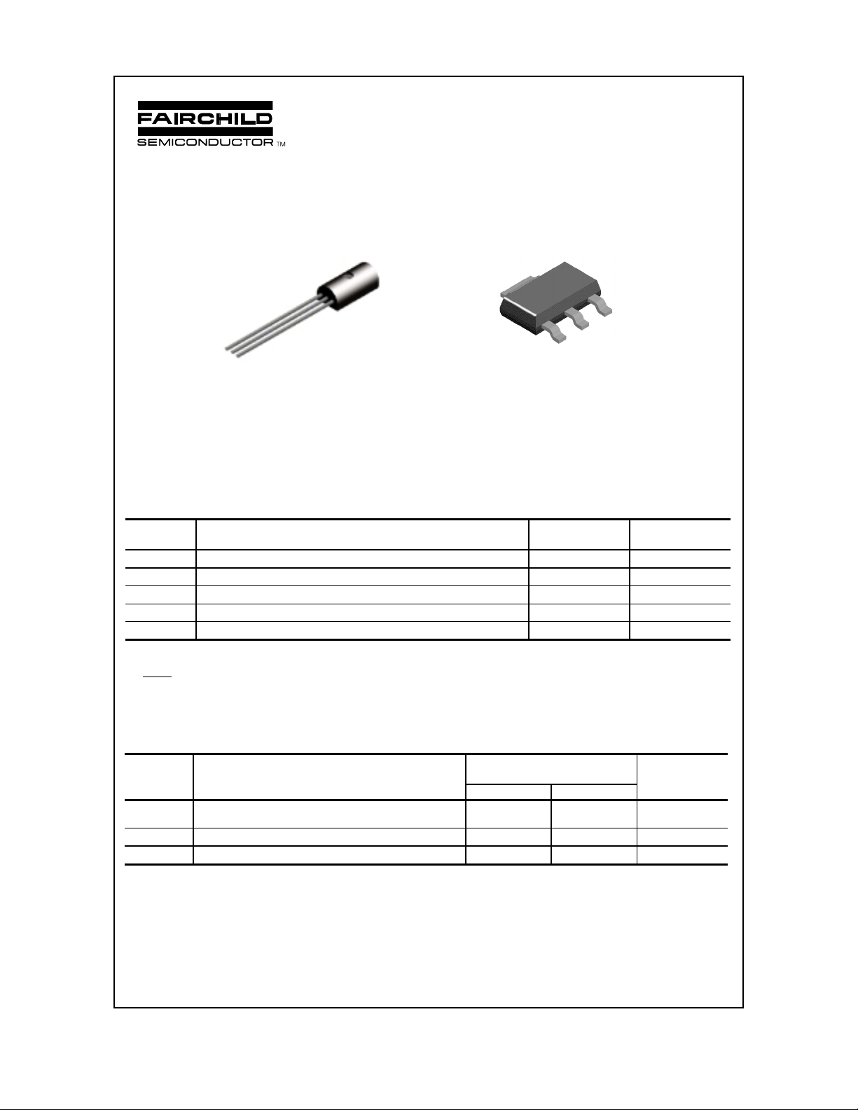
TN6714A / NZT6714
TN6714A
C
B
E
TO-226
NZT6714
C
E
C
B
SOT-223
NPN General Purpose Amplifier
This device is designed for general purpose medium power
amplifiers and switches requiring collector currents to 1.5 A.
Sourced from Process 37.
Absolute Maximum Ratings* TA = 25°C unless otherwise noted
Symbol Parameter Value Units
V
CEO
V
CBO
V
EBO
I
C
TJ, T
stg
*These ratings are limiting values above which the serviceability of any semiconductor device may be impaired.
NOTES:
1) These ratings are based on a maximum junction temperature of 150 degrees C.
2) These are steady state limits. The factory should be consulted on applications involving pulsed or low duty cycle operations.
Collector-Emitter Voltage 30 V
Collector-Base Voltage 40 V
Emitter-Base Voltage 5.0 V
Collector Current - Continuous 2.0 A
Operating and Storage Junction Temperature Range -55 to +150
C
°
Thermal Characteristics TA = 25°C unless otherwise noted
Symbol Characteristic Max Units
TN6714A *NZT6714
P
D
R
θ
JC
R
θ
JA
*Device mounted on FR-4 PCB 36 mm X 18 mm X 1.5 mm; mounting pad for the collector lead min. 6 cm
1997 Fairchild Semiconductor Corporation
Total Devi ce Dissipat ion
Derate above 25°C
Thermal Resistance, Junction to Case 50
Thermal Resistance, Junction to Ambient 125 125
1.0
8.0
1.0
8.0
2
.
W
mW/°C
C/W
°
C/W
°
µ
µ
NPN General Purpose Amplifier
(continued)
Electrical Characteristics TA= 25°C unless otherwise noted
Symbol Parameter Test Conditions Min Max Units
OFF CHARACTERISTICS
V
(BR)CEO
V
(BR)CBO
V
(BR)EBO
I
CBO
I
EBO
ON CHARACTERISTICS
h
FE
V
sat
CE(
V
BE(on)
SMALL SIGNAL CHARACTERISTICS
h
fe
C
cb
*Pulse T est: Pulse Width ≤ 300 µs, Duty Cycle ≤ 1.0%
Collector-Emitter Breakdown Voltage* IC = 10 mA, IB = 030V
Collector-Base Breakdown Voltage
Emitter-Base Breakdown Voltage
I
= 100 µA, IE = 0
C
I
= 100 µA, IC = 0
E
Collector-Cutoff Current VCB = 40 V, IE = 0 0.1
Emitte r-Cutoff Current VEB = 5.0 V, IC = 0 0.1
DC Current Gain IC = 10 mA, VCE = 1.0 V
I
= 100 mA, VCE = 1.0 V
C
I
= 1.0 A, VCE = 1.0 V
Collector-Emitter Saturation Voltag e IC = 1.0 A, IB = 100 mA 0.5 V
)
C
40 V
5.0 V
A
A
55
60
50 250
Base-Emitter On Vol t age IC = 1.0 A, VCE = 1.0 V 1.2 V
Small-Signal Current Gain IC = 50 mA, VCE = 10 V,
2.5 25
f = 20 MHz
Collector-Base Capacitance VCB = 10 mA, IE = 0, f = 1.0 MHz 30 pF
TN6714A / NZT6714
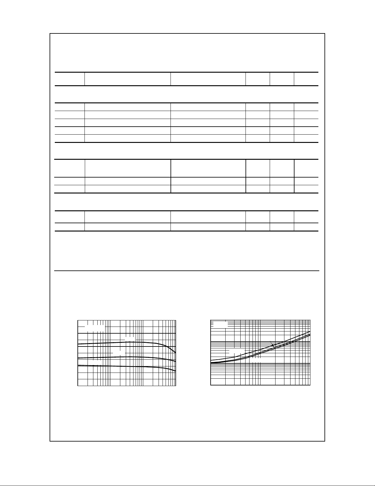
T ypical Characteristics
Typical Pulsed Curr e nt Gain
vs Collector Current
500
V = 5V
CE
125 °C
25 °C
- 40 °C
0
0.001 0.01 0.1 1
I - CO LLEC TOR CU RR ENT (A)
C
h - TYPI CAL PULSED CURR ENT GA IN
400
300
200
100
FE
Collector-Emi tt er Satu ration
V o lt age vs C o llec tor Cur rent
1
= 10
β
0.1
125 °C
0.01
0.01 0.1 1
CESAT
V - COLLECTOR-EMITTER VOLTAGE (V)
I - COLLECTOR CURRENT (A)
C
25 °C
- 4 0 °C
3
Typical Characteristics (continued)
TN6714A / NZT6714
NPN General Purpose Amplifier
(continued)
Base-Emitter Saturati o n
V o lta ge vs Co llecto r Cu r rent
β
1.4
= 10
1.2
1
- 40 °C
0.8
0.6
25 °C
125 °C
0.4
BESAT
0.2
V - BASE -EMI TTER VOLTAGE (V)
0.01 0.1 1
I - COLLE C TOR CURREN T (A)
C
Co lle ctor- Cuto f f Current
vs Ambien t Tem perature
100
V = 20V
CB
10
1
0.1
Base- Emitter ON Vo ltag e vs
Collector Current
1
0.8
0.6
0.4
0.2
BE(ON)
V - BASE-EMITTER ON VOLTAGE (V)
- 4 0 °C
25 °C
125 °C
V = 5V
CE
1 10 100 1000
I - COLLECTOR CURRENT (mA)
C
Collector-Base Capacitance
vs Collector-Base Vol tage
40
30
20
10
CBO
I - COLLECTOR CURRENT (nA)
25 50 75 100 125 150
T - AMBIEN T TEMPERATU RE ( C )
A
°
Gain Bandwidth Product
vs Collector Current
500
V = 10V
CE
400
300
200
100
0
1 10 100 1000
FE
h - GAIN BANDWIDTH PRODUCT (MHz)
I - COLLECTOR CURRENT (mA)
C
0
0 4 8 1216202428
OBO
V - COLL ECTOR -BASE VOLTAGE (V )
- COLLECTOR- BASE CAPACITANC E (p F )
CB
Safe Operating Area TO-226 / SOT-223
10
10
µ
1
*PULSED
0.1
OPERATION
T = 25 °C
A
C
I - COLLECTOR CURRENT (A)
0.01
110100
DC T = 25 °C
COLLEC TO R LEAD
DC T = 25 °C
AMBIENT
LIMIT DETERMINED
BY BV
V - COLLECTOR-EMITT ER VOLTAG E (V)
CE
100
CEO
S*
µ
S*
1.0 ms*
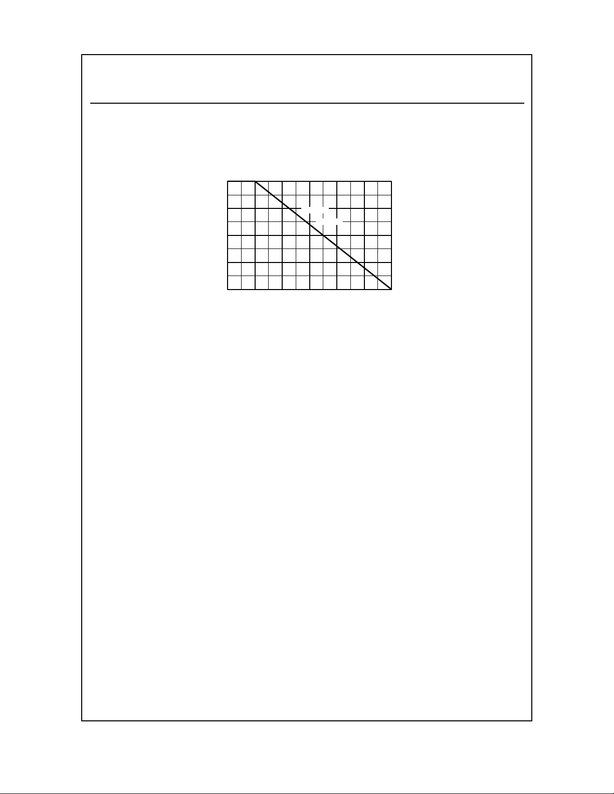
Typical Characteristics (continued)
Power Dissipation vs
Ambient T em perature
1
TN6714A / NZT6714
NPN General Purpose Amplifier
(continued)
0.75
0.5
0.25
D
P - POWER DISSIPATION (W)
0
0 25 50 75 100 125 150
TO-226
SOT-223
TEMPERATURE ( C)
o
3

TO-226AE Tape and Reel Data
TO-226AE Packagin g
Co nf ig u r atio n: Fi gur e 1.0
FSCINT Label sampl e
FAIRCHILDSEMICONDUCTOR CORPORATION
LOT:
CBVK741B019
NSID:
PN2222N
D/C1:
D9842
F63TNR Label sampl e
LOT: CBVK7 41B019
FSID: PN22 2N
D/C1: D9842 QTY1: SPEC REV:
D/C2: QTY2: CPN:
TO-226AE T NR/AMMO PACKING IN F ROMATION
Packing Style Quantity EOL code
Reel A 2,000 D26Z
Amm o M 2,000 D74Z
Unitweight = 0.300gm
Reel weig ht with c om po nents = 0.868 k g
Ammo weig ht with co mp on ents = 0.880k g
Max qu anti ty p er interm ediate box = 10,000 un it s
(TO-226AE) BULK PACKING INFORMATION
EOL CODE DESCRIPTION
J18Z
J05Z
NO EOL
CODE
SPEC REV:
QA REV:
E2,000 D27Z
P2,000 D75Z
TO-18 OPTION ST D NO L EAD CLIP
TO-5 OPTION STD NO LEAD CLIP
TO-226 STA NDARD
STRAIGHT
HTB:B
QTY:
10000
SPEC:
B2
(FSCINT)
QTY: 200 0
SPEC:
N/F: F (F63TNR)3
LEADCLIP
DIMENSION
NO L EA DCLIP
327mm x 158mm x 135mm
Immed i ate B o x
Cus tom i zed
Labe l
QUANTITY
1.0 K / B OX
1.0 K / B OX
1.5 K / B OX
TAPE and REEL OPTION
See Fig 2.0 for various
Reeling Styles
5 Reels per
Int er m ed i ate B o x
F63TNR
Labe l
Cus tom i zed
Labe l
AMMO PACK OPTION
See Fig 3.0 for 2 Ammo
Pack Options
5 Am m o box es per
Int er m ed i ate B o x
F63TNR
Bar c ode Label
BULK OPTION
SeeBulk Packing
Information table
FSCINT Barc ode Label
1,500 un i t s per
EO70 box for
std option
375mm x 267mm x 375mm
Int er m ed i ate B o x
333mm x 231mm x 183mm
Int er m ed i ate B o x
Anti-stat ic
Bub bl e Sheets
114mm x 102mm x 51mm
EO70 Im mediate B ox
FSCINT
Labe l
Cus tom i zed
Labe l
FSCINT
Labe l
Cus tom i zed
Labe l
530mm x 130mm x 83mm
Inter medi ate box
FSCINT Labe l
©2000 Fairchild Semiconductor International
Cus t omized
Label
7,500 un i t s m axi m u m
per interm edi at e box
for st d opt i o n
5EO70boxesper
Int er m ed i ate B o x
October 1999, Rev. A1

TO-226AE Tape and Reel Data, continued
TO-226AE Reeling Styl e
Configuration:
Figure 2.0
Machine Opt ion "A" (H)
Style "A" D2 6Z, D70Z (s /h)
TO-226AE Radial Ammo Packaging
Confi guration:
Figure 3.0
ORDER STY LE
D74Z (M )
FIRST WIRE OFF IS COL L ECT OR (ON PKG. 92)
ADHESIVE TAPE IS ON THE TOP SIDE
FLAT OF TRANSISTOR IS ON TOP
Machine Option "E" (J)
Style "E" D 2 7 Z, D71Z (s/ h)
FIRST WIRE OFF IS EMITTER (ON PKG. 92)
ADHESIVE TAPE IS ON THE TOP SIDE
FLAT OF TRANSISTOR IS ON BOTTOM
ORDER STY LE
D75Z (P)
FIRST WIRE OFF IS EMITTER
ADHESIVE TAPE IS ON BOTTOM SIDE
FLAT OF TRANSISTOR IS ON BOTTOM
FIRST WIRE OFF IS COL L ECT OR
ADHESIVE TAPE IS ON BOTTOM SIDE
FLAT OF TRANSISTOR IS ON TOP
October 1999, Rev. A1

TO-226AE Tape and Reel Data, continued
TO-226AE Tape and Reel Taping
DimensionConfiguration:
Figur e 4.0
Hb
H1
HO
TO-226AE Reel
Configuration:
P Pd
P1 F1
P2
PO
User D irectionof Feed
Figur e 5.0
Hd
b
d
L1
DO
S
L
ITEM DESCR I PT ION
Baseof Package to Lead Bend
Component Height
LeadC li nch He ig ht
Component BaseHeig ht
ComponentAlignment( s ide/ side)
ComponentAlignment( front/back )
Component Pitch
Feed H ole Pi t ch
HoleCenter to First Lead
HoleCenterto Component Center
Lead S pread
LeadThickness
Cut LeadLen gth
Taped Lead Lengt h
Taped LeadThickness
Carrier Tape Thicknes s
Carrier TapeWidth
Hold - down Tape Width
Hold- down Tape position
Feed HolePosition
SprocketHole Diameter
LeadS pri ng O ut
W1
WO
t
W2
W
t1
SYM BOL
b
Hb
HO
H1
Pd
Hd
P
PO
P1
P2
F1/F2
d
L
L1
t
t1
W
WO
W1
W2
DO
S
DIM ENSI ON
0.0 98 (ma x )
1.0 78 (+/- 0 .050 )
0.6 30 (+/- 0 .020 )
0.7 48 (+/- 0 .020 )
0.0 40 (ma x)
0.0 31 (ma x)
0.5 00 (+/- 0 .020 )
0.5 00 (+/- 0 .008 )
0.1 50 (+0. 0 09 , -0.01 0 )
0.2 47 (+/- 0 .007 )
0.1 04 (+/- 0 . 010)
0.0 18 (+0. 0 02 , -0.00 3)
0.4 29 (ma x)
0.2 09 (+0. 0 51, -0.05 2)
0.0 32 (+/- 0 .006 )
0.0 21 (+/- 0.006 )
0.7 08 (+0. 0 20, -0.01 9)
0.2 36 (+/- 0 .012 )
0.0 35 (ma x)
0.3 60 (+/- 0 .025 )
0.1 57 (+0. 0 08 , -0.00 7)
0.0 04 (ma x)
F63TNR Label
Customi zed Label
W2
ELECTROSTATIC
SENSIT IV ED EV ICES
D3
Note: All di mensions are in inches.
D4
D1
ITEM DESCRIPT ION SYMBOL MINIMUM MAXIMUM
D2
W1
W3
Reel Diameter D1 13.975 14.025
Ar bo r Hole Di a mete r (Stan dard) D2 1.160 1 .200
CoreDiameter D3 3.100 3.300
Hub RecessInnerDiameter D4 2.700 3.100
Hub Re cess Dept h W 1 0.370 0.570
Flangeto FlangeInner W idth W 2 1.630 1.690
Hu b to Hu b Cent e r W idth W 3 2.09 0
Note: All dimensions are inches
(Small Hole) D2 0.650 0.700
October 1999, Rev. A1

TO-226AE Package Dimensions
TO-226AE (FS PKG Code 95, 99)
S4.70-4.32;
1:1
Scale 1:1 on letter size paper
Dimensions shown below are in:
inches [millimeters]
Part Weight per unit (gram): 0.300
S1.52-1.02;
2" TYP
S7.87-7.37;
S15.61-14.47;
S0.51-0.36;
S0.76-
0.36;
S4.45-3.81;
1
S1.40-1.14;
S1.40-1.14;
32
5" TYP
S1.65-1.27;
0.51
2" TYP
S0.48-0.30;
99 95
PIN
1EE
2BC
3CB
TO-226AE (95,99)
S7.73-7.10;
S2.41-2.13;
©2000 Fairchild Semiconductor International
For leadformed option ordering,
refer to Tape & Reel data information.
October 1999, Rev. A1

SOT-223 Tape and Reel Data
SOT-223 Packaging
Configuration: Figure 1.0
Customized Label
F63TNR Label
Embossed Car rier Tape
Antistatic Cover Tape
Static Dissipative
Packaging Description:
SOT-223 parts are shipped in tape. The carrier tape is
made from a dissipative (carbon filled) polycarbonate
resin. The cover tape is a multilayer film (Heat Activated
Adhesive in nature) primarily composed of polyester film,
adhesive layer, sealant, and anti-static sprayed agent.
These reeled parts in standard option are shipped with
2,500 uni t s pe r 13" o r 33 0c m d ia met er reel . Th e reel s ar e
dark blue in color and is made of polystyrene plastic (antistatic coated). Other option comes in 500 units per 7" or
177cm di ameter reel. This and some o ther options are
further described in the Packaging Information table.
These full reels are individually barcode labeled and
placed inside a standard intermediate box (illustrated in
figure 1.0) made of recyclable corrugated brown paper.
One box contains two reels maximum. And these boxes
are placed inside a barcode labeled shipping box which
comes in di ff ere nt siz es depe nd in g on th e num be r of pa rts
shippe d.
SOT-223 Packaging Information
Packaging Option
Packaging type
Qty per Reel/Tube/Bag
Reel Size
Box Dimension (mm)
Max qty per Box
Weight per unit (gm)
Weight per Reel (kg)
Note/Comments
Standard
(no flow code)
13" Dia
343x64x343 184x187x47
0.1246 0.1246
0.7250 0.1532
D84Z
TNR
2,500 500
5,000 1,000
TNR
7" Dia
F63TNR Label
184mm x 184mm x 47mm
Pizza Box for D84Z Option
SOT-223 Tape Leader and Trailer
Configuration: Figure 2.0
F
014
852
F
014
852
SOT-223 Unit Orientation
343mm x 342mm x 64mm
Intermediate box for Standard
F
014
852
F
014
852
F63TNR Label sample
LOT: CBVK741B019
FSID: PN2222A
D/C1: D9842 QTY1: SPEC REV:
D/C2: QTY2: CPN:
F63TNR Label
QTY: 3000
SPEC:
N/F: F (F63TNR)3
Carrier Tape
Cover Tape
Trailer Tape
300mm minimum or
38 empty pockets
©2000 Fairchild Semiconductor International
Components
Leader Tape
500mm minimum or
62 empty pockets
September 1999, Rev. B

SOT-223 Tape and Reel Data, continued
SOT-223 Embossed Carrier Tape
Configuration: Figure 3.0
T
K0
Wc
B0
P0
D0
E1
F
W
E2
Tc
A0
D1
P1
User Direction of Feed
Dimensions are in millimeter
Pkg type
SOT-223
(12mm)
Notes: A0, B0, and K0 dimensions are determined with respect to the EIA/Jedec RS-481
SOT-223 Reel Configuration: Figure 4.0
A0 B0 W D0 D1 E1 E2 F P1 P0 K0 T Wc Tc
6.83
7.42
12.0
1.55
1.50
1.75
10.25
+/-0.10
+/-0.10
+/-0.3
+/-0.05
+/-0.10
+/-0.10
rotational and lateral movement requirements (see sketches A, B, and C).
B0
20 deg maximum component rotation
Sketch A (Side or Front Sectional View)
Component Rotation
5.50
min
+/-0.05
20 deg maximum
A0
Sketch B (Top View)
Component Rotation
W1 Measured at Hub
8.0
+/-0.1
Typical
component
cavity
center line
Typical
component
center line
Dim A
Max
4.0
+/-0.1
0.292
1.88
+/-0.10
0.5mm
maximum
Sketch C (Top View)
Component lateral movement
+/-
0.0130
9.5
+/-0.025
0.5mm
maximum
0.06
+/-0.02
Dim A
max
Tape Size
12mm 7" Dia
12mm 13" Dia
Reel
Option
Dim N
Diameter Option
7"
See detail AA
B Min
Dim C
13" Diameter Option
See detail AA
W2 max Measured at Hub
Dim D
W3
min
DETAIL AA
Dimensions are in inches and millimeters
Dim A Dim B Dim C Dim D Dim N Dim W1 Dim W2 Dim W3 (LSL-USL)
7.00
0.059
177.8
13.00
330
1.5
0.059
1.5
512 +0.020/-0.008
13 +0.5/-0.2
512 +0.020/-0.008
13 +0.5/-0.2
0.795
20.2
0.795
20.2
5.906
150
7.00
178
0.488 +0.078/-0.000
12.4 +2/0
0.488 +0.078/-0.000
12.4 +2/0
0.724
18.4
0.724
18.4
0.469 – 0.606
11.9 – 15.4
0.469 – 0.606
11.9 – 15.4
July 1999, Rev. B

SOT-223 Package Dimensions
SOT-223 (FS PKG Code 47)
1 : 1
Scale 1:1 on letter size paper
Part Weight per unit (gram): 0.1246
©2000 Fairchild Semiconductor International
September 1999, Rev. C

TRADEMARKS
The following are registered and unregistered trademarks Fairchild Semiconductor owns or is authorized to use and is
not intended to be an exhaustive list of all such trademarks.
ACEx™
Bottomless™
CoolFET™
CROSSVOLT™
DOME™
E2CMOS
EnSigna
TM
TM
FACT™
FACT Quiet Series™
FAST
FASTr™
GlobalOptoisolator™
GTO™
HiSeC™
ISOPLANAR™
MICROWIRE™
OPTOLOGIC™
OPTOPLANAR™
P ACMAN™
POP™
PowerTrench
QFET™
QS™
QT Optoelectronics™
Quiet Series™
SILENT SWITCHER
SMART ST ART™
SuperSOT™-3
SuperSOT™-6
SuperSOT™-8
SyncFET™
TinyLogic™
UHC™
VCX™
DISCLAIMER
FAIRCHILD SEMICONDUCTOR RESERVES THE RIGHT TO MAKE CHANGES WITHOUT FURTHER
NOTICE TO ANY PRODUCTS HEREIN T O IMPROVE RELIABILITY , FUNCTION OR DESIGN. FAIRCHILD
DOES NOT ASSUME ANY LIABILITY ARISING OUT OF THE APPLICA TION OR USE OF ANY PRODUCT
OR CIRCUIT DESCRIBED HEREIN; NEITHER DOES IT CONVEY ANY LICENSE UNDER ITS PA TENT
RIGHTS, NOR THE RIGHTS OF OTHERS.
LIFE SUPPORT POLICY
FAIRCHILD’S PRODUCTS ARE NOT AUTHORIZED FOR USE AS CRITICAL COMPONENTS IN LIFE SUPPORT
DEVICES OR SYSTEMS WITHOUT THE EXPRESS WRITTEN APPROVAL OF FAIRCHILD SEMICONDUCTOR CORPORA TION.
As used herein:
1. Life support devices or systems are devices or
systems which, (a) are intended for surgical implant into
the body, or (b) support or sustain life, or (c) whose
failure to perform when properly used in accordance
with instructions for use provided in the labeling, can be
reasonably expected to result in significant injury to the
user.
2. A critical component is any component of a life
support device or system whose failure to perform can
be reasonably expected to cause the failure of the life
support device or system, or to affect its safety or
effectiveness.
PRODUCT STA TUS DEFINITIONS
Definition of Terms
Datasheet Identification Product Status Definition
Advance Information
Preliminary
No Identification Needed
Obsolete
Formative or
In Design
First Production
Full Production
Not In Production
This datasheet contains the design specifications for
product development. Specifications may change in
any manner without notice.
This datasheet contains preliminary data, and
supplementary data will be published at a later date.
Fairchild Semiconductor reserves the right to make
changes at any time without notice in order to improve
design.
This datasheet contains final specifications. Fairchild
Semiconductor reserves the right to make changes at
any time without notice in order to improve design.
This datasheet contains specifications on a product
that has been discontinued by Fairchild semiconductor.
The datasheet is printed for reference information only.
Rev. G
 Loading...