Fairchild TL494 service manual

现货库存、技术资料、百科信息、热点资讯,精彩尽在鼎好!
TL494
SMPS Controller
www.fairchildsemi.com
Features
• Internal regulator provides a stable 5V reference supply
trimmed to 5%
• Uncommitted output TR for 200mA sink or so urce
current
• Output control fo r push-pull or single-ende d ope rat ion
• Variable duty cycle by dead time control (pin 4) Complete
PWM control circuit
• On-chip oscillator with master or slave operation
• Internal circuit prohibits double pulse at either output
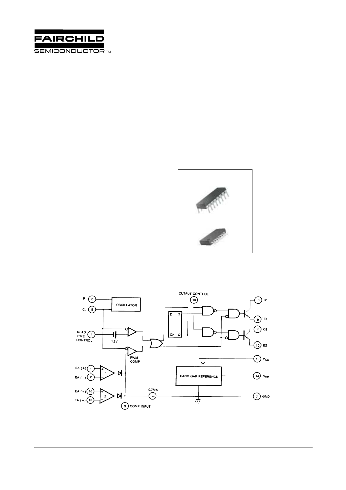
Internal Block Diagram
Description
The TL494 is used for the control circuit of the PWM
switching regul at or. The TL4 94 c ons i st s of 5V refe r e nc e
voltage circuit, two error amplifiers, flip flop, an output control circuit, a PWM comparator, a dead time comparator and
an oscillator. This device can be operated in the switching
frequency of 1 K Hz to 300 KHz.
16-DIP
1
16-SOP
1
©2000 Fairchild Semiconductor International
Rev. 5.0

TL494
Absolute Maximum Ratings
Parameter Symbol Value Unit
Supply Voltage V
Collector Supply Voltage V
Output Current I
Amplifier Input Voltage V
Power Dissipation (T
Operating Temperature Range T
Storage Temperature Range T
= 25°C) P
A
CC
C
O
IN
D
OPR
STG
42 V
42 V
250 mA
V
+ 0.3 V
CC
1 (TL494CN)
0.9 (TL494CD)
0 ~ +70 °C
-65 ~ + 150 °C
W
2

Electrical Characteristics
(VCC = 20V, f = 10KHz, TA = 0°C to + 70°C, unless otherwise specified)
Parameter Symbol Conditions Min. Typ. Max. Unit
REFERENCE SECTION
Reference Output Voltage V
Line Regulation ∆V
Temperature Coefficient of V
REF
Load Regulation ∆V
Short-Circuit Output Currnet I
∆V
REF
REF
REF
REF
SC
OSCILLATOR SECTION
Oscillation Frequency f C
Frequency Change with Temperature ∆f/∆TC
DEAD TIME CONTROL SECTION
Input Bias Current I
Maximum Duty Cycle D
Input Threshold Voltage V
BIAS
(MAX)
ITH
ERROR AMP SECTION
Input Offset Voltage V
Input Offset Current I
Input Bias Current I
Common Mode Input Voltage V
Open-Loop Voltage Gain G
IO
IO
BIAS
CM
VO
Unit-Gain Bandwidth BW - - 650 - KHz
PWM COMPARATOR SECTION
Input Threshold Voltage V
Input Sink Currnet I
ITH
SINK
OUTPUT SECTION
Output Saturation Voltage
Common Emitter
Common Collector V
Collector Off-State Currnet I
Emitter Off-State Current I
V
CE(SAT)VE
CC(SAT)VC
C(OFF)
E(OFF)
TOTAL DEVICE
Supply Current I
CC
OUTPUT SWITCHING CHARACTERISTIC
Rise Time t
R
Common Emitter - - - 100 200
Common Collector - - - 100 200
Fall Time t
F
Common Emitter - - - 25 100
Common Collector - - - 40 100
I
= 1mA 4.75 5.0 5.25 V
REF
VCC = 7V to 40V - 2.0 25 mV
/∆TTA = 0°C to 70°C - 0.01 0.03 %/°C
I
= 1mA to 10mA - 1.0 15 mV
REF
V
= 0V 10 35 50 mA
REF
= 0.01µF, RT = 12KΩ -10-KHz
T
= 0.01µF, RT = 12KΩ --2%
T
VCC = 15V, 0V≤V
VCC = 15V, V4 = 0V
O.C Pin = V
≤5.25V - -2.0 -10 µA
4
REF
45 - - %
Zero Duty Cycle - 3.0 3.3
Max. Duty Cycle 0 - -
V3 = 2.5V - 2.0 10 mV
V3 = 2.5V - 25 250 mA
V3 = 2.5V - 0.2 1.0 µA
7V ≤ V
0.5V ≤ V
≤ 40V -0.3 - V
CC
≤3 .5V 70 95 - dB
3
CC
Zero Duty Cycle - 4 4.5 V
V3=0.7V -0.3 -0.7 - mV
= 0, IC = 200mA - 1.1 1.3
= 15V, IE = -200mA - 1.5 2.5
VCC = 40V, VCE = 40V - 2 100
VCC = VC = 40V, VE = 0 - - -100
Pin 6 = V
, VCC = 15V - 6 10 mA
REF
- ----
- ----
TL494
V
V
V
µA
ns
ns
3
 Loading...