

www.fairchildsemi.com
AN-9068
Gate Resistor Design Guidelines for SupreMOS® MOSFETs
Summary
The faster switching of power MOSFETs enables higher
power conversion efficiency. However, parasitic
components in the devices and boards are involving
switching characteristics more as the switching speed
increases. This creates unwanted side effects, like voltage
spikes or poor EMI performance. To achieve balance, it is
important to have optimized gate drive circuitry because a
power MOSFET is a gate-controlled device. One of critical
control parameters in gate-drive design is external series
gate resistor (R
maximum values of R
hard-switching applications. As too small R
). This note suggests minimum and
g
for the SupreMOS® MOSFETs in
g
results in
g
excessive dv/dt across drain and source of the MOSFET
during switching-off, low limit is a value that makes
switching dv/dt within the specification in the datasheets.
Silicon Carbide (SiC) Schottky barrier diode, Deuxpeed
rectifier, and STEALTH™2 diodes are used for clamp diode
since the diode characteristics affect the dv/dt. Too large R
causes loss and poor efficiency; therefore, the upper limit is
chosen to have the same switching losses as the SuperFET
MOSFETs or competitors.
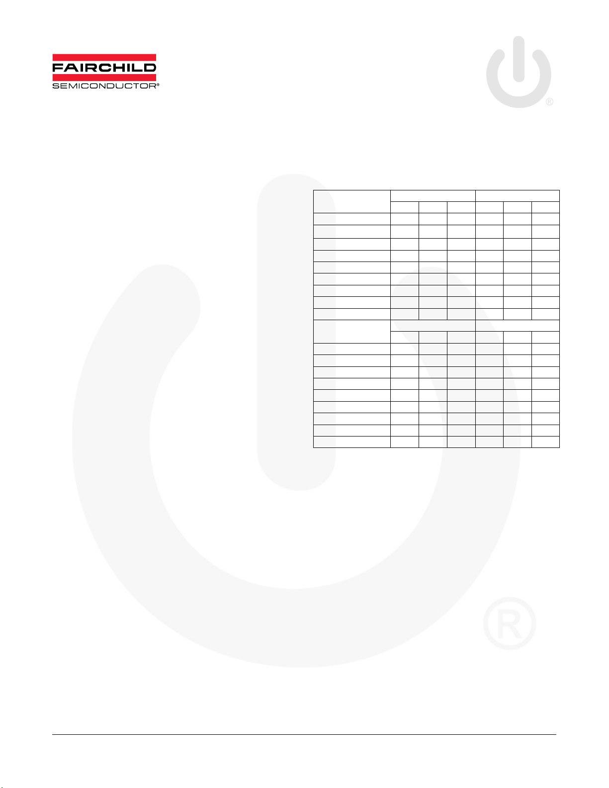
Minimum Values According to dv/dt
Table 1 shows low limits of Rg. The unit of Rg in Table 1 is
Ohm (). Since the dv/dt varies by drain current level, it is
tested with two conditions. For example, when using
FCP76N60N with a SiC diode under half of rated current, at
least 13 or larger R
dv/dt under 50V/ns during switching-off transient.
The dv/dt with a SiC diode is lower than dv/dt with other
diodes due to the bigger junction capacitance of SiC SBD.
A gap of the dv/dt values is getting larger at lower drain
current level and smaller R
current, the dv/dt is relatively low and the effect of output
capacitance of the MOSFET and diode junction capacitance
on the dv/dt becomes more significant.
If a specific R
value is needed for other dv/dt not shown in
g
Table 1, it can be selected by referring to Figure 13 through
Figure 18.
is required to keep the switching
g
. This is because, at lower
g
Table 1. Minimum Rg Guidelines Ohms
R
at 1/2 of Id
g
FCP9N60N 0 0 0 0 33 36
FCP11N60N
FCP13N60N 0 0 0 27 36 39
FCP16N60N 0 0 6.8 27 33 36
FCP22N60N 0 13 18 27 36 39
FCP25N60N 0 13 18 22 36 36
FCA36N60N 6.8 13 16 22 33 36
FCA47N60N 6.8 11 13 22 27 27
FCA76N60N 6.8 6.8 6.8 13 16 16
Rg at Rated Id
FCP9N60N 6.8 13 18 27 43 47
FCP11N60N 6.8 13 18 27 36 39
®
g
®
FCP13N60N 10 16 22 30 43 47
FCP16N60N 10 13 18 27 36 39
FCP22N60N 10 16 22 30 43 47
FCP25N60N 13 16 18 27 39 43
FCA36N60N 13 16 18 22 36 39
FCA47N60N 11 13 13 16 27 27
FCA76N60N 6.8 6.8 10 13 18 18
dv/dt<100V/ns dv/dt<50V/ns
SiC Dx S2 SiC Dx S2
0 0 0 0
dv/dt<100V/ns dv/dt<50V/ns
SiC Dx S2 SiC Dx S2
Upper Limits Considering Switching
Losses
When the SuperFET® MOSFET or other previousgeneration power MOSFET is directly replaced with the
SupreMOS MOSFET, switching losses are reduced, but the
dv/dt may be higher. To control the dv/dt of SupreMOS
MOSFETs, increased R
should be a limit line for increasing the R
losses with SupreMOS MOSFET could be larger. Figure 19
through Figure 54 show switching losses acco rd ing to R
each device. R
for similar or less switching loss can be
g
raised. For example, if 10 is used for a FCA35N60
SuperFET MOSFET, 33 achieves similar E
under conditions of half of rated drain current and
STEALTH™2 diode.
is required. In this case, there
g
or switching
g
and E
ON
33 36
for
g
in
OFF
© 2009 Fairchild Semiconductor Corporation www.fairchildsemi.com
Rev. 1.0.3 • 4/6/11
AN-9068 APPLICATION NOTE
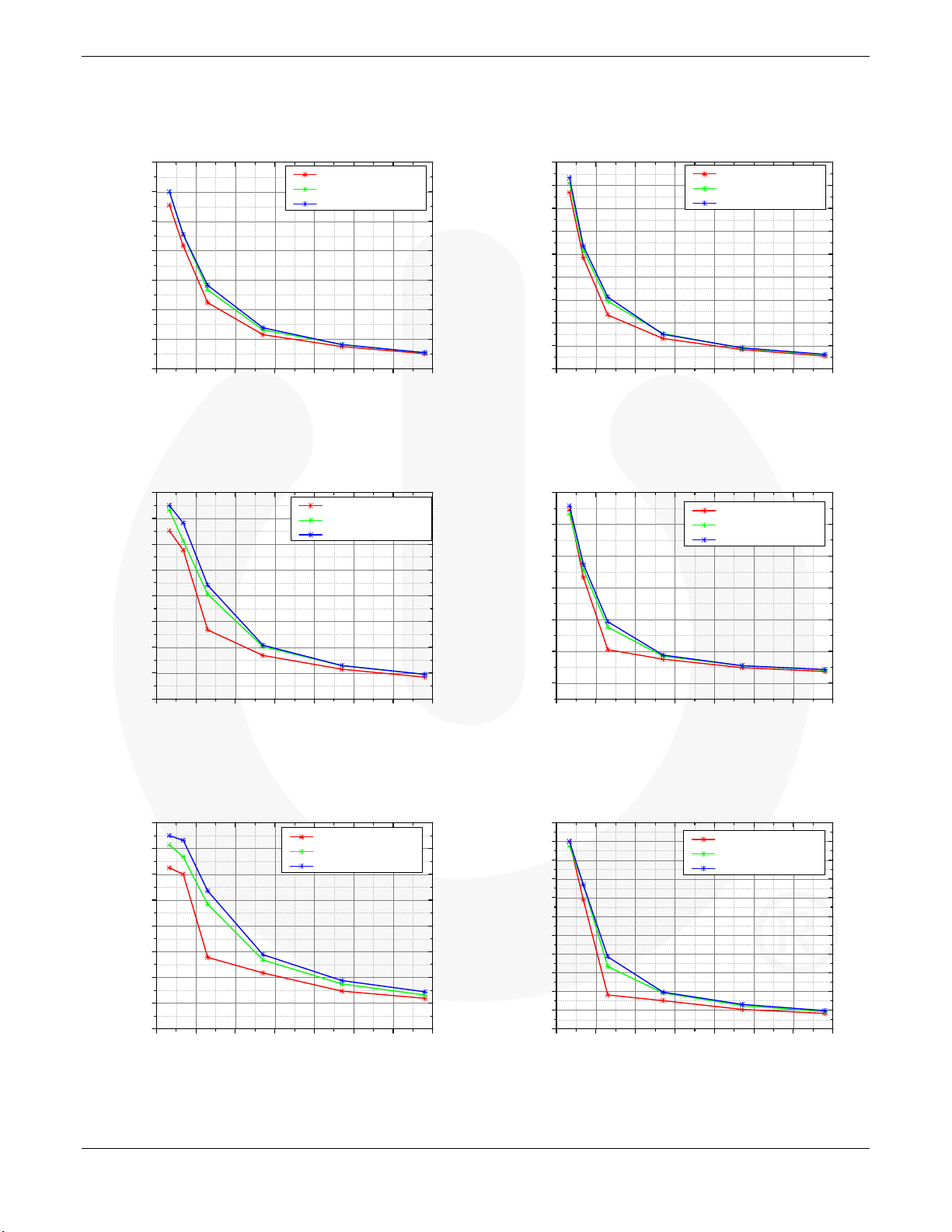
Typical Performance Characteristics
140
w/ SiC SBD
1/2 of Id
120
w/ Deuxpeed®rectifier
w/ STEALTHTM 2 diode
100
80
60
dv/dt [V/ns]
40
20
0
0 10203040506070
Rg (Ohm)
Figure 1. FCA76N60N dv/dt at Half I
160
140
120
100
80
60
dv/dt [V/ns]
40
20
0
0 10203040506070
1/2 of Id
w/ SiC SBD
w/ Deuxpeed®rectifier
w/ STEALTHTM 2 diode
Rg (Ohm)
D
180
160
140
120
100
80
dv/dt [V/ns]
60
40
20
0
0 10203040506070
w/ SiC SBD
w/ Deuxpeed®rectifier
w/ STEALTHTM 2 diode
Rg (Ohm)
Id
Figure 2. FCA76N60N dv/dt at Rated I
300
250
200
150
100
dv/dt [V/ns]
50
0
0 10203040506070
Id
w/ SiC SBD
w/ Deuxpeed®rectifier
w/ STEALTHTM 2 diode
Rg (Ohm)
D
Figure 3. FCA47N60N dv/dt at Half I
160
140
120
100
80
60
dv/dt [V/ns]
40
20
0
0 10203040506070
1/2 of Id
w/ SiC SBD
w/ Deuxpeed®rectifier
w/ STEALTHTM 2 diode
Rg (Ohm)
D
Figure 5. FCA36N60N dv/dt at Half I
D
Figure 4. FCA47N60N dv/dt at Rated I
330
300
270
240
210
180
150
120
dv/dt [V/ns]
90
60
30
0
0 10203040506070
Figure 6. FCA36N60N dv/dt at Rated I
D
Id
w/ SiC SBD
w/ Deuxpeed®rectifier
w/ STEALTHTM 2 diode
Rg (Ohm)
D
© 2009 Fairchild Semiconductor Corporation www.fairchildsemi.com
Rev. 1.0.3 • 4/6/11 2
AN-9068 APPLICATION NOTE
Typical Performance Characteristics
160
140
120
100
80
60
dv/dt [V/ns]
40
20
0
0 10203040506070
w/ SiC SBD
w/ Deuxpeed® rectifier
w/ STEALTHTM2 diode
Rg (Ohm)
Figure 7. FCP25N60N dv/dt at Half I
1/2 of Id
130
120
110
100
90
80
70
dv/dt [V/ns]
60
50
40
30
20
0 10203040506070
1/2 of Id
w/ SiC SBD
w/ Deuxpeed®rectifier
w/ STEALTHTM2 diode
Rg [Ohm]
350
300
w/ SiC SBD
w/ Deuxpeed® rectifier
w/ STEALTHTM2 diode
Id
250
200
150
dv/dt [V/ns]
100
50
0
0 10203040506070
Rg (Ohm)
D
Figure 8. FCP25N60N dv/dt at Rated I
D
Id
200
180
160
140
120
100
80
dv/dt [V/ns]
60
40
20
0
0 10203040506070
w/ SiC SBD
w/ Deuxpeed®rectifier
w/ STEALTHTM diode
Rg [Ohm]
Figure 9. FCP22N60N dv/dt at Half I
120
100
80
60
dv/dt [V/ns]
40
20
0
0 10203040506070
1/2 of Id
w/ SiC SBD
w/ Deuxpeed®rectifier
w/ STEALTHTM2 diode
Rg [Ohm]
Figure 11. FCP16N60N dv/dt at Half I
D
D
Figure 10.FCP22N60N dv/dt at Rated I
200
180
160
140
120
100
80
dv/dt [V/ns]
60
40
20
0
0 10203040506070
Id
w/ SiC SBD
w/ Deuxpeed®rectifier
w/ STEALTHTM diode
Rg [Ohm]
Figure 12.FCP16N60N dv/dt at Rated I
D
D
© 2009 Fairchild Semiconductor Corporation www.fairchildsemi.com
Rev. 1.0.3 • 4/6/11 3
AN-9068 APPLICATION NOTE
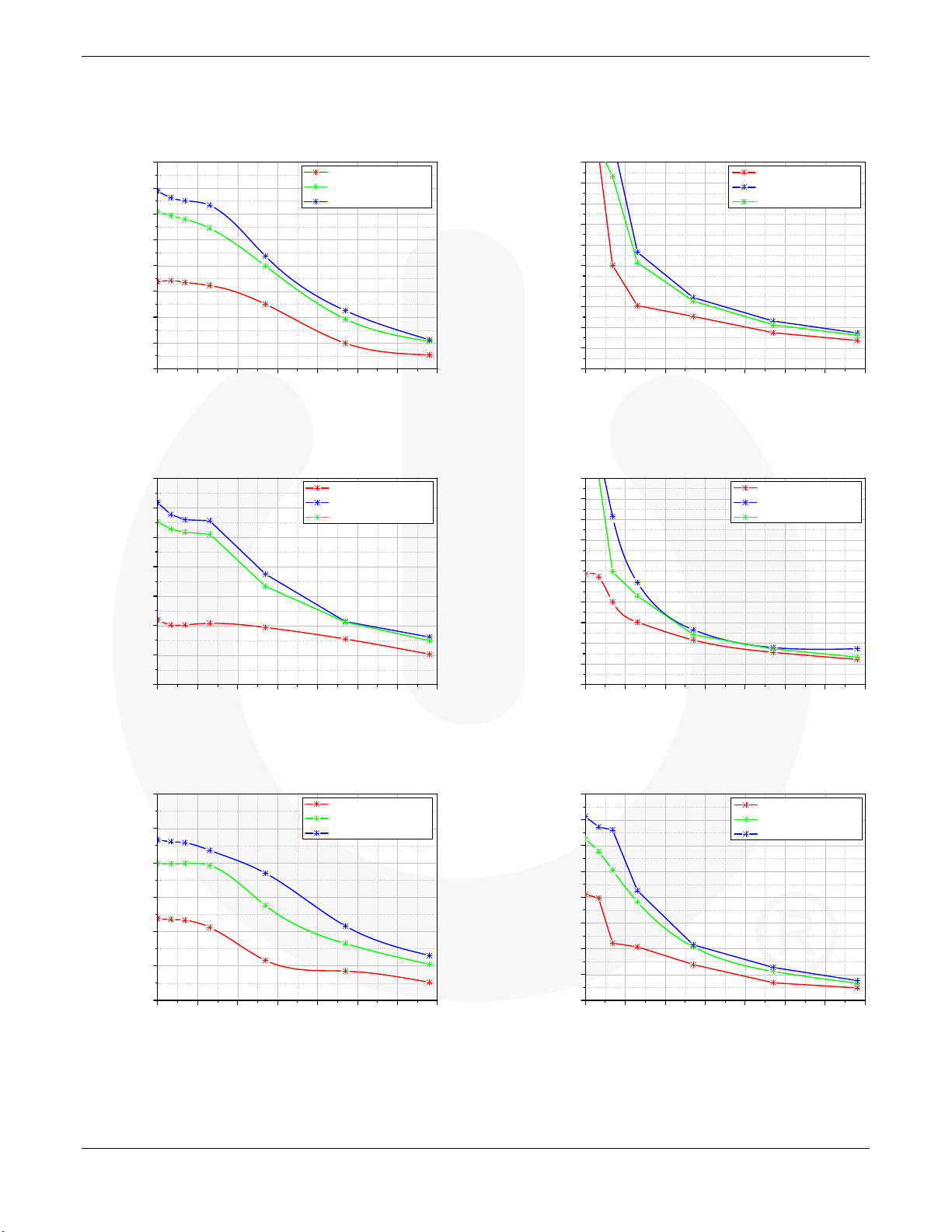
Typical Performance Characteristics
100
90
80
70
60
dv/dt [V/ns]
50
40
30
20
0 10203040506070
w/ SiC SBD
w/ Deuxpeed®rectifier
w/ STEALTHTM2 diode
Rg [Ohm]
Figure 13. FCP13N60N dv/dt at Half I
1/2 of Id
80
70
60
50
40
dv/dt [V/ns]
30
20
10
0 10203040506070
1/2 of Id
w/ SiC SBD
w/ Deuxpeed®rectifier
w/ STEALTHTM2 diode
Rg [Ohm]
200
180
160
140
120
100
80
dv/dt [V/ns]
60
40
20
0
0 10203040506070
w/ SiC SBD
w/ Deuxpeed®rectifier
w/ STEALTHTM2 diode
Rg [Ohm]
Id
D
Figure 14.FCP13N60N dv/dt at Rated I
D
Id
200
180
160
140
120
100
80
dv/dt [V/ns]
60
40
20
0
0 10203040506070
w/ SiC SBD
w/ Deuxpeed®rectifier
w/ STEALTHTM2 diode
Rg [Ohm]
Figure 15. FCP11N60N dv/dt at Half I
80
70
60
50
dv/dt [V/ns]
40
30
20
0 10203040506070
Figure 17. FCP9N60N dv/dt at Half I
1/2 of Id
w/ SiC SBD
w/ Deuxpeed®rectifier
w/ STEALTHTM2 diode
Rg [Ohm]
D
D
Figure 16.FCP11N60N dv/dt at Rated I
180
160
140
120
100
dv/dt [V/ns]
80
60
40
20
0 10203040506070
Id
w/ SiC SBD
w/ Deuxpeed®rectifier
w/ STEALTHTM2 diode
Rg [Ohm]
Figure 18.FCP9N60N dv/dt at Rated I
D
D
© 2009 Fairchild Semiconductor Corporation www.fairchildsemi.com
Rev. 1.0.3 • 4/6/11 4

AN-9068 APPLICATION NOTE
Typical Performance Characteristics
800
700
600
500
400
Eon [uJ]
300
200
100
0
FCA76N60N with STEALTHTM2 diode
45mOhm competitor with STEALTHTM2 diode
FCA76N60N with SiC SBD
45mOhm competitor with SiC SBD
0 10203040506070
Rg, Gate Resistor [Ohm]
Figure 19. FCA76N60N EON vs. Competitor at Half I
1/2 of Id
1800
1600
1400
1200
1000
800
Eoff[uJ]
600
400
200
FCA76N60N with STEALTHTM2 diode
45mOhm competitor with STEALTHTM2 diode
FCA76N60N with SiC SBD
45mOhm competitor with SiC SBD
0 10203040506070
Figure 21. FCA76N60N E
1/2 of Id
Rg, Gate Resistor [Ohm]
vs. Competitor at Half I
OFF
2000
1800
1600
1400
1200
Eon [uJ]
1000
800
600
400
0 10203040506070
FCA76N60N with STEALTHTM2 diode
45mOhm competitor with STEALTHTM2 diode
FCA76N60N with SiC SBD
45mOhm competitor with SiC SBD
Rg, Gate Resistor [Ohm]
Id
D
Figure 20.FCA76N60N EON vs. Competitor at Rated I
Id
4500
4000
3500
3000
2500
Eoff[uJ]
2000
1500
1000
FCA76N60N with STEALTHTM2 diode
45mOhm competitor with STEALTHTM2 diode
FCA76N60N with SiC SBD
45mOhm competitor with SiC SBD
0 10203040506070
Rg, Gate Resistor [Ohm]
D
D
Figure 22.FCA76N60N E
vs. Competitor at Rated I
OFF
D
800
700
600
500
400
Eon [uJ]
300
200
100
0
FCA47N60N with STEALTH
FCA47N60 with STEALTH
FCA47N60N with SiC SBD
FCA47N60 with SiC SBD
0 10203040506070
TM
TM
2 diode
2 diode
Rg, Gate Resistor [Ohm]
1/2 of Id
2000
1800
1600
1400
1200
1000
800
Eon [uJ]
600
400
200
0
FCA47N60N with STEALTH
FCA47N60 with STEALTH
FCA47N60N with SiC SBD
FCA47N60 with SiC SBD
0 10203040506070
Rg, Gate Resistor [Ohm]
TM
Id
TM
2 diode
2 diode
Figure 23. FCA47N60N EON vs. FCA47N60 at Half I
D
© 2009 Fairchild Semiconductor Corporation www.fairchildsemi.com
Rev. 1.0.3 • 4/6/11 5
Figure 24.FCA47N60N EON vs. FCA47N60 at Rated I
D

AN-9068 APPLICATION NOTE
A
Typical Performance Characteristics
1400
FCA47N60N with STEALTH
1200
1000
800
600
Eoff [uJ]
400
200
0
FCA47N60 with STEALTH
FCA47N60N with Si C SBD
FCA47N60 with SiC SBD
0 10203040506070
TM
TM
2 diode
2 diode
Rg, Gate Resistor [Ohm]
1/2 of Id
Figure 25. FCA47N60N E
vs. FCA47N60 at Half I
OFF
1/2 of Id
500
450
400
350
300
250
200
Eon[uJ]
150
100
FCA36N60N with STEALTH
FCA35N60 with STEALTH
99mOhm competitor with STEALTH
FCA36N60N with SiC SBD
FCA35N60 with SiC SBD
99mOhm competitor with SiC SBD
50
0
0 10203040506070
TM
TM
2 diode
2 diode
TM
2 diode
Rg, Gate Resistor [Ohm]
3500
3000
FCA47N60N with STEALTH
FCA47N60 with STEALTH
FCA47N60N with SiC SBD
TM
TM
2 diode
2 diode
FCA47N60 with SiC SBD
Id
2500
2000
Eoff [uJ]
1500
1000
500
0 10203040506070
Rg, Gate Resistor [Ohm]
D
Figure 26.FCA47N60N E
vs. FCA47N60 at Rated I
OFF
D
Id
1400
1200
1000
800
600
Eon[uJ]
400
200
FCA36N60N with STEALTH
FCA35N60 with STEALTH
99mOhm competitor with STEALTH
FCA36N60N with SiC SBD
FCA35N60 with SiC SBD
99mOhm competitor with SiC SBD
0
0 10203040506070
TM
TM
2 diode
2 diode
TM
2 diode
Rg, Gate Resistor [Ohm]
Figure 27. FCA36N60N EON vs. FCA35N60
and Competitor at Half I
700
600
500
400
300
Eoff[uJ]
200
100
FCA36N60N with STEALTH
FCA35N60 with STEALTH
99mOhm competitor with STEALTH
FCA36N60N with SiC SBD
FCA35N60 with SiC SBD
99mOhm competitor with SiC SBD
0
0 10203040506070
Figure 29. FCA36N60N E
1/2 of Id
TM
2 diode
TM
2 diode
TM
2 diode
Rg, Gate Resistor [Ohm]
vs. FCA35N60
OFF
and Competitor at Half I
D
D
Figure 28.FCA36N60N E
and Competitor at Rated I
1800
1600
1400
1200
1000
800
Eoff[uJ]
600
400
200
FCA36N60N with STEALTH
FCA35N60 with STEALTH
99mOhm competitor with STEALTH
FCA36N60N with SiC SBD
FCA35N60 with SiC SBD
99mOhm competitor with SiC SBD
0
0 10203040506070
Figure 30.FC
TM
TM
2 diode
Rg, Gate Resistor [Ohm]
36N60N E
and Competitor at Rated I
vs. FCA35N60
ON
Id
2 diode
TM
2 diode
OFF
D
vs. FCA35N60
D
© 2009 Fairchild Semiconductor Corporation www.fairchildsemi.com
Rev. 1.0.3 • 4/6/11 6

AN-9068 APPLICATION NOTE
Typical Performance Characteristics
160
140
120
100
80
Eon[uJ]
60
40
20
0
0 10203040506070
FCP25N60N with STEALTH
125mOhm competitor with STEALTH
FCP25N60N with SiC SBD
125mOhm competitor with SiC SBD
TM
2 diode
TM
2 diode
Rg, Gate Resistor [Ohm]
Figure 31. FCP25N60N EON vs. Competitor at Half I
1/2 of Id
140
120
100
80
60
Eoff[uJ]
40
20
0
FCP25N60N with STEALTH
125mOhm competitor with STEALTH
FCP25N60N with SiC SBD
125mOhm competitor with SiC SBD
0 10203040506070
1/2 of Id
TM
2 diode
TM
2 diode
Rg, Gate Resistor [Ohm]
350
300
250
200
150
Eon[uJ])
100
50
0
0 10203040506070
FCP25N60N with STEALTH
125mOhm competitor with STEALTH
FCP25N60N with SiC SBD
125mOhm competitor with SiC SBD
TM
2 diode
TM
2 diode
Rg, Gate Resistor [Ohm]
Id
D
Figure 32.FCP25N60N EON vs. Competitor at Rated I
D
Id
500
450
400
350
300
250
200
Eoff[uJ]
150
100
50
0
FCP25N60N with STEALTH
125mOhm competitor with STEALTH
FCP25N60N with SiC SBD
125mOhm competitor with SiC SBD
0 10203040506070
TM
2 diode
TM
2 diode
Rg, Gate Resistor [Ohm]
Figure 33. FCP25N60N E
120
100
Eon[uJ]
FCP22N60N with STEALTHTM2 diode
165mOhm competitor with STEALTHTM2 diode
FCP22N60N with SiC SBD
165mOhm competitor with SiC SBD
80
60
40
20
0
0 10203040506070
Rg, Gate Resistor [Ohm]
vs. Competitor at Half I
OFF
1/2 of Id
D
Figure 34.FCP25N60N E
vs. Competitor at Rated I
OFF
Id
280
240
200
160
120
Eon[uJ]
FCP22N60N with STEALTHTM2 diode
165mOhm competitor with STEALTHTM2 diode
FCP22N60N with SiC SBD
165mOhm competitor with SiC SBD
80
40
0
0 10203040506070
Rg, Gate Resistor [Ohm]
Figure 35. FCP22N60N E
© 2009 Fairchild Semiconductor Corporation www.fairchildsemi.com
Rev. 1.0.3 • 4/6/11 7
vs. Competitor at Half I
ON
D
Figure 36.FCP22N60N EON vs. Competitor at Rated I
D
D

AN-9068 APPLICATION NOTE
Typical Performance Characteristics
120
100
FCP22N60N with STEALTHTM2 diode
165mOhm competitor with STEALTHTM2 diode
FCP22N60N with SiC SBD
165mOhm competitor with SiC SBD
80
60
Eoff[uJ]
1/2 of Id
40
20
0
0 10203040506070
Rg, Gate Resistor [Ohm]
Figure 37. FCP22N60N E
vs. Competitor at Half I
OFF
1/2 of Id
120
100
Eon[uJ]
FCP16N60N with STEALTHTM2 diode
FCP20N60 with STEALTHTM2 diode
199mOhm competitor with STEALTHTM2 diode
FCP16N60N with SiC SBD
FCP20N60 with SiC SBD
199mOhm competitor with SiC SBD
80
60
40
20
360
320
280
240
200
Eoff[uJ]
160
120
FCP22N60N with STEALTHTM2 diode
165mOhm competitor with STEALTHTM2 diode
FCP22N60N with SiC SBD
165mOhm competitor with SiC SBD
80
40
0 10203040506070
Rg, Gate Resistor [Ohm]
Id
D
Figure 38.FCP22N60N E
vs. Competitor at Rated I
OFF
D
Id
280
240
200
160
Eon[uJ]
120
FCP16N60N with STEALTHTM2 diode
FCP20N60 with STEALTHTM2 diode
199mOhm competitor with STEALTHTM2 diode
FCP16N60N with SiC SBD
FCP20N60 with SiC SBD
199mOhm competitor with SiCSBD
80
40
0
0 10203040506070
Rg, Gate Resistor [Ohm]
Figure 39. FCP16N60N E
vs. FCP20N60
ON
and Competitor at Half I
160
140
120
100
Eoff[uJ]
FCP16N60N with STEALTHTM2 diode
FCP20N60 with STEALTHTM2 diode
199mOhm competitor with STEALTHTM2 diode
FCP16N60N with SiC SBD
FCP20N60 with SiC SBD
199mOhm competitor with SiC SBD
80
60
40
20
0
0 10203040506070
Figure 41. FCP16N60N E
1/2 of Id
Rg, Gate Resistor [Ohm]
vs. FCP20N60
OFF
and Competitor at Half I
0
0 10203040506070
Rg, Gate Resistor [Ohm]
Figure 40.FCP16N60N E
D
and Competitor at Rated I
vs. FC P20N6 0
ON
D
Id
360
320
280
240
200
160
Eoff[uJ]
120
FCP16N60N with STEALTHTM2 diode
FCP20N60 with STEALTHTM2 diode
199mOhm competitor with STEALTHTM2 diode
FCP16N60N with SiC SBD
FCP20N60 with SiC SBD
199mOhm competitor with SiC SBD
80
40
0
0 10203040506070
Rg, Gate Resistor [Ohm]
Figure 42.FCP16N60N E
D
and Competitor at Rated I
vs. FCP20N60
OFF
D
© 2009 Fairchild Semiconductor Corporation www.fairchildsemi.com
Rev. 1.0.3 • 4/6/11 8

AN-9068 APPLICATION NOTE
Typical Performance Characteristics
90
FCP13N60N with STEALTHTM2 diode
FCP16N60 with STEALTHTM2 diode
FCP13N60N with SiC SBD
75
FCP16N60 with SiC SBD
60
45
Eon[uJ]
1/2 of Id
30
15
0
0 10203040506070
Rg, Gate Resistor [ohm]
Figure 43. FCP13N60N E
vs. FCP16N60 at Half I
ON
1/2 of Id
90
FCP13N60N with STEALTHTM2 diode
FCP16N60 with STEALTHTM2 diode
FCP13N60N with SiC SBD
75
FCP16N60 with SiC SBD
60
45
Eoff[uJ]
30
180
FCP13N60N with STEALTHTM2 diode
FCP16N60 with STEALTHTM2 diode
FCP13N60N with SiC SBD
150
FCP16N60 with SiC SBD
120
90
Eon[uJ]
60
30
0
0 10203040506070
Rg, Gate Resistor [Ohm]
Id
D
Figure 44.FCP13N60N EON vs. FCP16N60 at Rated I
D
Id
200
FCP13N60N with STEALTHTM2 diode
FCP16N60 with STEALTHTM2 diode
FCP13N60N with SiC SBD
FCP16N60 with SiC SBD
160
120
Eoff[uJ]
80
15
0
0 10203040506070
Rg, Gate Resistor [Ohm]
Figure 45. FCP13N60N E
vs. FCP16N60 at Half I
OFF
1/2 of Id
45
40
35
30
25
20
Eon[uJ]
15
10
5
0
0 10203040506070
FCP11N60N with STEALTHTM2 diode
299mOhm competitor with STEALTHTM2 diode
FCP11N60N with SiC SBD
299mOhm competitor with SiC SBD
Rg, Gate Resistor [Ohm]
Figure 47. FCP11N60N E
vs. Competitor at Half I
ON
40
0
0 10203040506070
Rg, Gate Resistor [Ohm]
D
Figure 46.FCP13N60N E
vs. FCP16N60 at Rated I
OFF
D
Id
120
100
Eon[uJ]
FCP11N60N with STEALTHTM2 diode
299mOhm competitor with STEALTHTM2 diode
FCP11N60N with SiC SBD
299mOhm competitor with SiC SBD
80
60
40
20
0
0 10203040506070
Rg, Gate Resistor [Ohm]
D
Figure 48.FCP11N60N EON vs. Competitor at Rated I
D
© 2009 Fairchild Semiconductor Corporation www.fairchildsemi.com
Rev. 1.0.3 • 4/6/11 9

AN-9068 APPLICATION NOTE
Typical Performance Characteristics
30
25
20
Eoff[uJ]
15
10
FCP11N60N with STEALTHTM2 diode
299mOhm competitor with STEALTHTM2 diode
FCP11N60N with SiC SBD
299mOhm competitor with SiC SBD
5
0 10203040506070
Rg, Gate Resistor [Ohm]
1/2 of Id
Figure 49. FCP11N60N E
vs. Competitor at Half I
OFF
1/2 of Id
70
FCP9N60N with STEALTHTM2 diode
FCP11N60 with STEALTHTM2 diode
60
385mOhm competitor with STEALTHTM2 diode
FCP9N60N with SiC SBD
FCP11N60 with SiC SBD
50
385mOhm competitor with SiC SBD
40
30
Eon[uJ]
20
100
Eoff[uJ]
FCP11N60N with STEALTHTM2 diode
299mOhm competitor with STEALTHTM2 diode
FCP11N60N with SiC SBD
80
299mOhm competitor with SiC SBD
60
40
20
0
0 10203040506070
Rg, Gate Resistor [Ohm]
Id
D
Figure 50.FCP11N60N E
vs. Competitor at Rated I
OFF
D
Id
120
100
Eon[uJ]
FCP9N60N withSTEALTHTM2 diode
FCP11N60 with STEALTHTM2 diode
385mOhm competitor with STEALTHTM2 diode
FCP9N60N with SiC SBD
FCP11N60 with SiC SBD
385mOhm competitor with SiC SBD
80
60
40
10
0
0 10203040506070
Rg, Gate Resistor [Ohm]
Figure 51. FCP9N60N E
and Competitor at Half I
vs. FCP11N60
ON
D
1/2 of Id
50
FCP9N60N with STEALTHTM2 diode
FCP11N60 with STEALTHTM2 diode
385mOhm competitor with STEALTHTM2 diode
40
FCP9N60N with SiC SBD
FCP11N60 with SiC SBD
385mOhm competitor with SiC SBD
30
Eoff[uJ]
20
10
0
0 10203040506070
Rg, Gate Resistor [Ohm]
Figure 53. FCP9N60N E
and Competitor at Half I
vs. FCP11N60
OFF
D
20
0
0 10203040506070
Rg, Gate Resistor [Ohm]
Figure 52.FCP9N60N E
and Competitor at Rated I
vs. FC P11N60
ON
D
Id
120
100
Eoff[uJ]
FCP9N60N with STEALTHTM2 diode
FCP11N60 with STEALTHTM2 diode
385mOhm competitor with STEALTHTM2 diode
FCP9N60N with SiC SBD
FCP11N60 with SiC SBD
385mOhm competitor with SiC SBD
80
60
40
20
0
0 10203040506070
Rg, Gate Resistor [Ohm]
Figure 54.FCP9N60N E
and Competitor at Rated I
vs. FC P11N6 0
OFF
D
© 2009 Fairchild Semiconductor Corporation www.fairchildsemi.com
Rev. 1.0.3 • 4/6/11 10

AN-9068 APPLICATION NOTE
Related Datasheets
FCA76N60N – 600V N-Channel SupreMOS® MOSFET
FCH76N60N – 600V N-Channel SupreMOS
FCH76N60NF– 600V N-Channel Supr eMO S
FCH47N60N– 600V N-Channel SupreMOS
FCH47N60NF– 600V N-Channel Supr eMO S
FCB36N60N – 600V N-Channel SupreMOS
FCP36N60N – 600V N-Channel SupreMOS
FCA36N60NF – 600V N-Channel SupreMOS
FCH25N60N – 600V N-Channel SupreMOS
FCP25N60N_F102 – 600V N-Channel SupreMOS
FCI25N60N_F102 – 600V N-Channel SupreMOS
FCP22N60N – 600V N-Channel SupreMOS
FCPF22N60NT – 600V N-Channel SupreMOS
FCA22N60N – 600V N-Channel SupreMOS
FCH22N60N – 600V N-Channel SupreMOS
FCP16N60N – 600V N-Channel SupreMOS
FCPF16N60NT – 600V N-Channel SupreMOS
FCA16N60N – 600V N-Channel SupreMOS
FCP13N60N- 600V N-Channel SupreMOS
FCPF13N60NT – 600V N-Channel SupreMOS
FCP11N60N – 600V N-Channel SupreMOS
FCPF11N60NT – 600V N-Channel SupreMOS
FCP9N60N – 600V N-Channel SupreMOS
FCPF9N60NT – 600V N-Channel SupreMOS
FCD9N60NTM – 600V N-Channel SupreMOS
®
MOSFET
®
MOSFET
®
MOSFET
®
MOSFET
®
MOSFET
®
MOSFET
®
MOSFET
®
MOSFET
®
®
MOSFET
®
MOSFET
®
MOSFET
®
MOSFET
®
MOSFET
®
MOSFET
®
MOSFET
®
MOSFET
®
MOSFET
®
MOSFET
®
MOSFET
®
MOSFET
®
MOSFET
®
MOSFET
®
MOSFET
MOSFET
DISCLAIMER
FAIRCHILD SEMICONDUCTOR RESERVES THE RIGHT TO MAKE CHANGES WITHOUT FURTHER NOTICE TO ANY PRODUCTS
HEREIN TO IMPROVE RELIABILITY, FUNCTION, OR DESIGN. FAIRCHILD DOES NOT ASSUME ANY LIABILITY ARISING OUT OF THE
APPLICATION OR USE OF ANY PRODUCT OR CIRCUIT DESCRIBED HEREIN; NEITHER DOES IT CONVEY ANY LICENSE UNDER ITS
PATENT RIGHTS, NOR THE RIGHTS OF OTHERS.
LIFE SUPPORT POLICY
FAIRCHILD’S PRODUCTS ARE NOT AUTHORIZED FOR USE AS CRITICAL COMPONENTS IN LIFE SUPPORT DEVICES OR SYSTEMS
WITHOUT THE EXPRESS WRITTEN APPROVAL OF THE PRESIDENT OF FAIRCHILD SEMICONDUCTOR CORPORATION.
As used herein:
1. Life support devices or systems are devices or systems
which, (a) are intended for surgical implant into the body, or
(b) support or sustain life, or (c) whose failure to perform
when properly used in accordance with instructions for use
provided in the labeling, can be reasonably expected to
result in significant injury to the user.
2. A critical component is any component of a life support
device or system whose failure to perform can be reasonably
expected to cause the failure of the life support device or
system, or to affect its safety or effectiveness.
© 2009 Fairchild Semiconductor Corporation www.fairchildsemi.com
Rev. 1.0.3 • 4/6/11 11
 Loading...