

Page 1
www.fairchildsemi.com
SPT5240
10-bit, 400 MWPS Current Output
Digital-to-Analog Converter
Features
• 400 MWPS update rate
• Complementary current outputs
• +3.3 V power supply
• Low power dissipation:
149mW (typ) @ƒ
• Excellent AC performance:
SFDR = 58dBc for ƒ
• Internal reference
= 400MHz and 12mA output
CLK
= 400MHz and ƒ
CLK
Applications
• Battery-operated devices
• Portable RF devices
• Set top boxes
• Video displays
• Broadband RF
• High-speed test equipment
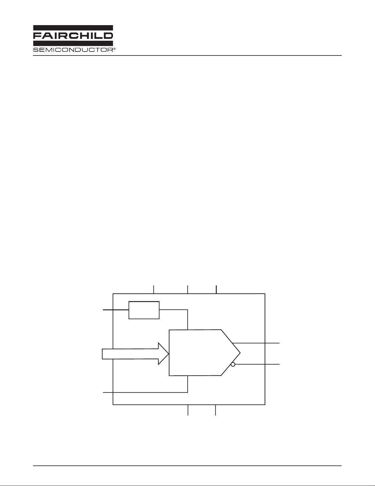
Functional Block Diagram
= 1.27 MHz
OUT
PWD
Description
The SPT5240 is a 10-bit digital-to-analog converter that
performs at an update rate of 400M words per second. The
architecture achieves excellent high-frequency performance
with very low power dissipation. This makes it ideal for all
types of battery-operated equipment requiring high-speed
digital-to-analog conversion.
The SPT5240 operates over an extended industrial
temperature range from -40°C to +85°C and is available in a
32-lead LQFP package.
DV
DD
AV
DD
I
SET
D0 – D9
CLK
10 Bits
Reference
Circuit
10-bit
Current Output
DAC
DGND AGND
IO
IO
P
N
REV. 1 June 2003
Page 2

(
DATA SHEET SPT5240
Electrical Specifications
T
= 25°C, AV
A
I
= 20mA, R
OUT
Parameter Conditions Test Level Min Typ Max Units
DC Performance
Resolution 10 Bits
Differential Linearity Error (DLE) DC at IO
Integral Linearity Error (ILE) DC at IO
Offset Error DC at both outputs I -.005 +.005 %FS
Full Scale Error DC at both outputs I -15 +15 %FS
Gain Error DC at both outputs I -15 +15 %FS
Maximum Full Scale Output Current V 30 mA
Output Compliance Voltage V 1.5 V
Output Impedance Full-scale output V 250 k
Gain Error Tempco V ±300 ppm
AC Performance
Maximum Clock Rate IV 400
Glitch Energy Major code transition V 7 pV-s
Settling Time (t
Output Rise Time V 1.3 ns
Output Fall Time V 1.5 ns
Output Delay Time (t
Spurious Free Dynamic Range (SFDR)
Total Harmonic Distortion (THD) V -55 dBc
Digital and Clock Data Input
V
Minimum V 2 V
IH
V
Maximum V 1 V
IL
Logic “1” Current I -10 +10 µ A
Logic “0” Current I -10 +10 µ A
Input Setup Time (t
Input Hold Time (t
Clock Feedthrough V -29 dBFS
= 3.3V, DV
DD
= 50 Ω ; unless otherwise noted)
L
) See Figure 1, major code trans. V 7.5 ns
settling
D
= 3.3V,
DD
ƒ
= 1.27MHz,
OUT
ƒ
= 400MHz, Clock Duty Cycle = 50%,
CLK
N
N
I-1 2LSB
I-4±1.34 4 LSB
) See Figure 1 V 1.8 ns
V58dBc
) See Figure 1 V 1 ns
S
) See Figure 1 V 1 ns
H
Ω
FS/°C
MHz
TEST LEVEL CODES
All electrical characteristics are subject to the following conditions:
All parameters having min/max specifications are guaranteed. The Test Level column indicates the specific device testing
actually performed during production and Quality Assurance inspection.
LEVEL TEST PROCEDURE
I 100% production tested at the specified temperature.
IV Parameter is guaranteed by design or characterization data.
V Parameter is a typical value for information purposes only.
2
REV. 1 June 2003
Page 3
(
SPT5240 DATA SHEET
Electrical Specifications
T
= 25°C, AV
A
I
= 20mA, R
OUT
= 3.3V, DV
DD
= 50 Ω ; unless otherwise noted)
L
= 3.3V,
DD
(Continued)
ƒ
= 1.27MHz,
OUT
ƒ
= 400MHz, Clock Duty Cycle = 50%,
CLK
Parameter Conditions Test Level Min Typ Max Units
Power Supply Requirements
Supply Voltage AV
DD
= DV
DD
IV 3.0 +3.3 3.6 V
Supply Current Sleep Mode
AV
DD
DV
DD
Power Dissipation 20mA I
25MHz Clock V 9.5 mA
25MHz Clock V 200
IV 170 195 215 mW
V 149 mW
12mA I
OUT
OUT
µ A
TEST LEVEL CODES
All electrical characteristics are subject to the following conditions:
All parameters having min/max specifications are guaranteed. The Test Level column indicates the specific device testing
actually performed during production and Quality Assurance inspection.
LEVEL TEST PROCEDURE
I 100% production tested at the specified temperature.
IV Parameter is guaranteed by design or characterization data.
V Parameter is a typical value for information purposes only.
REV. 1 June 2003
3
Page 4

DATA SHEET SPT5240
Absolute Maximum Ratings
(beyond which the device may be damaged)
Parameter Min Max Units
Supply Voltage
AV
DV
DD
DD
3.7 V
3.7 V
Voltage Difference between AGND and DGND -0.5 0.5 V
Voltage Difference between AV
and DV
DD
DD
-0.5 0.5 V
Input Voltages
D0 – D9 -0.5 DV
CLK -0.5 DV
+0.5 V
DD
+0.5 V
DD
Junction Temperature 150 °C
Lead, soldering (10 seconds) 260 °C
Storage Temperature -65 +150 °C
Thermal Resistance ( Θ
Note:
Operation at any Absolute Maximum Rating is not implied. See Electrical Specifications for proper
nominal applied conditions in typical applications.
) for 32 lead LQFP 64 °C/W
JA
4
REV. 1 June 2003
Page 5

(
SPT5240 DATA SHEET
Typical Performance Characteristics
T
= 25°C, AV
A
I
= 20mA, R
OUT
= 3.3V, DV
DD
= 50 Ω ; unless otherwise noted)
L
= 3.3V,
DD
ƒ
= 1.27MHz,
OUT
ƒ
= 400MHz, Clock Duty Cycle = 50%,
CLK
AC Performance vs. Clock Frequency
65
60
55
50
45
dB
40
35
30
25
0 100 200 300 400 500 600
THD
SNR
Clock Frequency (MHz)
AC Performance vs. V
65
SFDR
THD
SNR
dB
60
55
50
45
40
DD
SFDR
AC Performance vs. Temperature
65
60
55
SFDR
THD
Clock frequency = 327MHz
dB
50
45
40
SNR
-50 -25 0 25 50 75
Temperature (°C)
Intergral Nonlinearity vs. Code
2.0
1.5
1.0
LSB's
0.5
0
35
3.0 3.3 3.6
VDD (V)
Differential Nonlinearity vs. Code
0.6
0.4
0.2
0
LSB's
-0.2
-0.4
-0.6
0 128 256 384 512 640 768 896 1024
Code
-0.5
0 128 256 384 512 640 768 896 1024
Code
AVDD, DVDD vs. Clock Frequency
45
35
25
AV
DD
mA
15
DV
5
DD
40
105 205 245 328 400
Clock (MHz)
REV. 1 June 2003
5
Page 6

DATA SHEET SPT5240
Specification Definitions
Differential Linearity Error (DLE) or
Differential Nonlinearity (DNL)
In an ideal DAC, output transitions between two adjacent
codes are 1 LSB apart. Differential Linearity Error is the
deviation, expressed in LSBs, from this ideal value.
Integral Linearity Error (ILE) or
Integral Nonlinearity (INL)
The ideal transfer for a DAC is a straight line drawn between
"zero-scale" output and "full-scale" output. ILE is the
deviation of the output from the straight line. The deviation
of the output at each code is measured and compared to the
ideal output at that code. ILE may also be expressed as a
sum of DLE starting from code 0…0 to the code that ILE
measurement is desired.
Monotonic
A digital-to-analog converter is considered monotonic if
the analog output never decreases as the code value at the
input increases. A DLE less than -1 LSB would indicate a
non-monotonic DAC.
Offset Error
The deviation, from ideal, at the DAC output when set to
zero-scale. In the current output DAC there should be no
current flow at zero-scale. Therefore, Offset Error is the
amount of current measured with the DAC set to zero-scale.
Full-Scale Error
The ideal maximum full-scale current output of the DAC is
determined by the value of R
deviation of the output from ideal with the offset error
included.
Gain Error
The ideal maximum full-scale current output of the DAC is
determined by the value of R
of the output from ideal with the offset error removed.
Full-Scale Output
The maximum current output available for a given value of
R
. In the SPT5240 IOP is full-scale at code 1111111111
SET
and IO
is full-scale at code 0000000000.
N
Zero-Scale Output
The minimum current output, ideally zero amps. In the
SPT5240 IO
is zero-scale at code 1111111111.
is zero-scale at code 0000000000 and IO
P
. Full-scale error is the
SET
. Gain error is the deviation
SET
N
Compliance Voltage
The maximum terminal output voltage for which the device
will provide the specified current output characteristics.
Harmonic
1. Of a sinusoidal wave, an integer multiple of the frequency
of the wave. Note: The frequency of the sine wave is called
the fundamental frequency or the first harmonic, the
second harmonic is twice the fundamental frequency,
third harmonic is three times the fundamental frequency, etc.
2. Of a periodic signal or other periodic phenomenon, such
as an electromagnetic wave or a sound wave, a component
frequency of the signal that is an integer multiple of the
fundamental frequency.
is the reciprocal of the period of the periodic phenomenon.
Note:
The fundamental frequency
the
Total Harmonic Distortion (THD)
The ratio of the sum of the power of first 9 harmonics above
the fundamental frequency to the power of the fundamental
frequency. Usually expressed in dBc.
Spurious Free Dynamic Range (SFDR)
The ratio of the fundamental sinusoidal power to the power
of the single largest harmonic or spurious signal within the
range of the 9th harmonic.
Clock Feedthrough
The ratio of the full-scale output to the peak-to-peak noise
generated at the DAC output by input clock transitions.
Expressed in dBFS.
Major Code Transition
The DAC code transition between 011…1 and 100…0 is
referred to as major code transition. This transition often
involves maximum number of internal circuit elements to
switch states, resulting in worst DLE, ILE, glitch, etc.
Glitch Energy
A glitch is a switching transient that appears in the output of
a DAC during a code transition. Glitch energy is measured as
a product of the output voltage and time duration for major
code transition, expressed in pV-s.
Output Rise Time
The amount of time for the output to change from 10%
to 90% of the full-scale voltage, for a positive full scale
transition from zero-scale to full-scale.
Output Fall Time
The amount of time for the output to change from 90%
to 10% of the full-scale voltage, for a negative full scale
transition from full-scale to zero-scale.
6
REV. 1 June 2003
Page 7

SPT5240 DATA SHEET
Pin Configuration Pin Assignments
D2
D1
DV
D0
DGND
CLK
DGND
AGND
DD
D3
DV
D4
DGND
32
31
30
29
1
2
3
DD
4
5
6
7
8
SPT5240SIT
32-pin LQFP
9
10
11
DD
AV
IO
AGND
12
P
AGND
DD
DV
D7
D6
D5
28
27
26
25
24
D8
23
DGND
22
D9
21
DGND
20
PWD
19
AV
DD
18
AGND
17
I
SET
13
14
15
16
N
AGND
AV
DD
N/C
IO
Theory of Operation
The SPT5240 is a 10-bit 400 MWPS digital-to-analog
converter. It integrates a DAC core with a bandgap reference
and operates from a +3.3V power supply.
Analog Outputs
IO
P
DAC current output. Full-scale output at 11…11
input code.
IO
N
Complementary current output. Full-scale output
at 00…00 input code.
Digital Inputs
D0 – D9 Digital inputs (D0 = LSB).
PWD Power down mode pin. Active high. Internally
pulled down.
CLK Clock input pin. Data is latched on the rising edge.
Reference
I
SET
Full-scale adjust control. Connection for
reference-current setting resistor.
Power
AGND Analog Supply Ground.
DGND Digital Supply Ground.
AV
DV
DD
DD
Analog +3.3V supply.
Digital +3.3V supply.
N/C No Connect
outputs of the decoders are latched using a second bank
of master-slave latches whose outputs then drive differential
current switches, which steer the appropriate current to
the IO
or ION outputs.
P
The DAC architecture is a compound differential current
output DAC consisting of a 6-bit fully segmented DAC for
the MSBs and a 4-bit fully segmented DAC for the LSBs.
The input cell, followed by a master-slave latch, buffers the
digital inputs. A 6:64 decoder decodes the digital data for
the MSBs, and a 4:16 decoder does so for the LSBs. The
N N+1
CLK
t
H
N
N-1
Digital
Inputs
VO
VON
t
S
P
The analog (AVDD) and digital (DVDD) power supplies are
separated on chip to allow flexibility in the interface board.
The analog (AGND) and digital (DGND) are separated on
chip. Circuit board ground planes should be separated and
tied together with a ferrite bead.
N+1 N+3
t
D
N+2
1 LSB
N
N+1N-2
1 LSB
REV. 1 June 2003
NOTE: Not to scale. For definition purposes only.
Figure 1: Timing Diagram
t
settling
7
Page 8

DATA SHEET SPT5240
Clock In
10-bit
Data Bus
0.01µF
0.1µF
10µF
+D3.3V
I
OUT
Adjust
Sleep
Mode
Select
R
SET
CLK I
SET
PWD
IO
P
SPT5240
IO
DD
DVDDDGND
AGND
AV
0.01µF
0.1µF
++
FB
10µF
+A3.3V
N
Notes:
1. FB = Ferrite Bead across analog and digital ground planes.
Place as close to DAC as feasible.
2. Minimum resistance (R
in maximum current output.
3. PWD pin has an internal pull-down resistor.
Set pin high to initate sleep mode.
4. Outputs (IO
VO
P
50Ω
50Ω
VO
N
) from I
SET
and ION) require minimum 5Ω load.
P
to ground relsults
SET
Figure 2: Typical Interface Circuit Diagram
Typical Interface Circuit
The SPT5240 requires few external components to achieve
the stated performance. Figure 2 shows the typical interface
requirements when used in normal circuit operation. The
following sections provide descriptions of the major
functions and outline performance criteria to consider for
achieving optimal performance.
Digital Inputs
The SPT5240 has a 10-bit-wide parallel data input designed
to work at +3.3V CMOS levels. Fast edges and low
transients provide for improved performance.
Clock Input
The SPT5240 is driven by a single-ended clock circuit. In
order to achieve best performance at the highest throughput,
a clock generation circuit should provide fast edges
and low jitter.
Input Protection
All I/O pads are protected with an on-chip protection circuit.
This circuit provides robust ESD protection in excess of
3,000 volts, in human body model, without sacrificing speed.
Power Supplies and Grounding
The SPT5240 may be operated in the range of 3.0 to 3.6
volts. Normal operation is recommended to be separate
analog and digital supplies operating at +3.3 volts. All
power supply pins should be bypassed as close to the
package as possible with the smallest capacitor closest to
the device. Analog and digital ground planes should be
connected together with a ferrite bead as shown in Figure 2
and as close to the DAC as possible.
Sleep Mode
To conserve power, the SPT5240 incorporates a power down
function. This function is controlled by the signal on
pin PWD. When PWD is set high, the SPT5240 enters the
sleep mode. The analog outputs are both set to zero current
output, resulting in less than 10mA current draw from
the analog supply. For minimum power dissipation, data
and clock inputs should be set to logic low or logic high.
Reference
The SPT5240 utilizes an on-chip bandgap reference to set
full-scale output current level. The current reference to the
DAC circuitry is set by the external resistance value between
the I
pin and analog ground.
SET
8 REV. 1 June 2003
Page 9

SPT5240 DATA SHEET
Analog Outputs
The SPT5240 provides differential current outputs which
provide an output level based on the value of R
SET
at
maximum output code (see Figure 3). The required value of
R
may be calculated using the formulas:
SET
LSB = IFS/1023
Then:
R
= 1.111 – (1000 • LSB)
SET
4 • LSB
Where IFS is the desired full-scale current output.
Each output requires a minimum 5Ω load to analog ground.
The typical circuit utilizes 50Ω loads to develop voltage for
the output transformer (refer to EB5240 data sheet).
Table 1: Input Data Format
Input Code D9 – D0 Analog Output
IO
0000000000 F
N
S
IO
P
0
35
R
Steps = 2.75kΩ
SET
30
25
(mA)
20
OUT
I
15
10
5
0
60.3 11.2
R
Value (kΩ)
SET
Figure 3: R
SET
vs. I
OUT
1111111111 0 F
Sleep XXXXXXXXXX 0 0
X indicates either data state.
Package Dimensions
LQFP-32
A
B
C D
E
F
S
G
H
Symbol Min Max Min Max
A 0.346 0.362 8.80 9.20
B 0.272 0.280 6.90 7.10
C 0.346 0.362 8.80 9.20
D 0.272 0.280 6.90 7.10
E 0.031 Typ 0.80 BSC
F 0.012 0.016 0.30 0.40
G 0.053 0.057 1.35 1.45
H 0.002 0.006 0.05 0.15
I 0.037 0.041 0.95 1.05
J 0.007 0.17
I
J
K0° 7° 0° 7°
L 0.020 0.030 0.50 0.75
INCHES MILLIMETERS
K
L
REV. 1 June 2003 9
Page 10

SPT5240 DATA SHEET
Ordering Information
Model Part Number Package Container Pack Qty
SPT5240 SPT5240SIT 32-pin LQFP Tray –
Temperature range for all parts: -40°C to +85°C.
DISCLAIMER
FAIRCHILD SEMICONDUCTOR RESERVES THE RIGHT TO MAKE CHANGES WITHOUT FURTHER NOTICES TO ANY PRODUCTS HEREIN TO IMPROVE RELIABILITY, FUNCTION
OR DESIGN. FAIRCHILD DOES NOT ASSUME ANY LIABILITY ARISING OUT OF THE APPLICATION OR USE OF ANY PRODUCT OR CIRCUIT DESCRIBED HEREIN; NEITHER DOES
IT CONVEY ANY LICENSE UNDER ITS PATENT RIGHTS, NOR THE RIGHTS OF OTHERS.
LIFE SUPPORT POLICY
FAIRCHILD’S PRODUCTS ARE NOT AUTHORIZED FOR USE AS CRITICAL COMPONENTS IN LIFE SUPPORT DEVICES OR SYSTEMS WITHOUT THE EXPRESS WRITTEN
APPROVAL OF THE PRESIDENT OF FAIRCHILD SEMICONDUCTOR CORPORATION. As used herein:
1. Life support devices or systems are devices or systems which, (a) are intended for
surgical implant into the body, or (b) support or sustain life, and (c) whose failure to per
form when properly used in accordance with instructions for use provided in the labeling,
can be reasonably expected to result in a significant injury of the user.
2. A critical component in any component of a life support device or system whose failure
to perform can be reasonably expected to cause the failure of the life support device or
system, or to affect its safety or effectiveness.
www.fairchildsemi.com © 2003 Fairchild Semiconductor Corporation
 Loading...