

Page 1
SMCJ5.0(C)A - SMCJ170(C)A
Features
• Glass passivated junction.
• 1500 W Peak Pulse Power capability
on 10/1000 µs waveform.
• Excellent clamping capability .
• Low incremental surge resistance.
• Fast response time; typically less
than 1.0 ps from 0 volts to BV for
unidirectional and 5.0 ns for
bidirectional.
• Typical I
• UL certified, UL #E210467.
less than 1.0 µA above 10V.
R
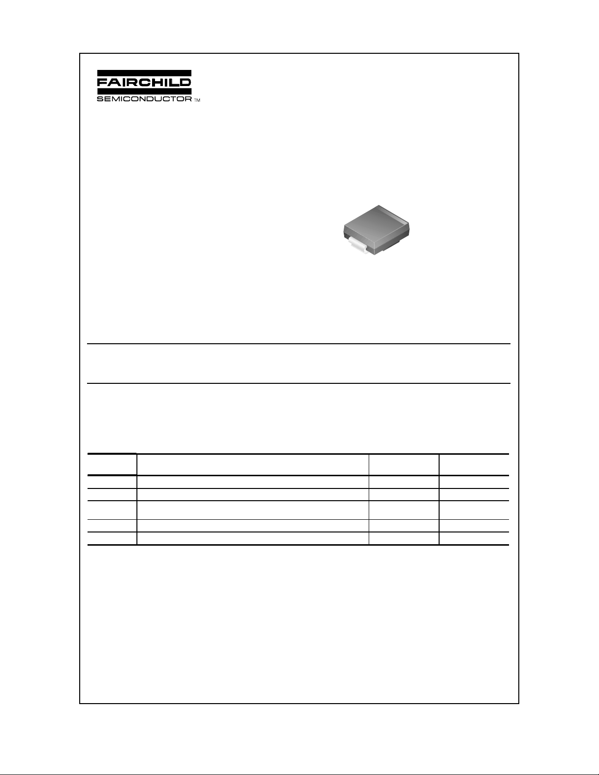
SMC/DO-214AB
COLOR BAND DENOTES CATHODE
ON UNIDIRECTIONAL DEVICES ONLY.
NO COLOR BAND ON BIDIRECTIONAL
DEVICES.
SMCJ5.0(C)A - SMCJ170(C)A
DEVICES FOR BIPOLAR APPLICA TIONS
- Bidirectional types use CA suffix.
- Electrical Characteristics apply in both directions.
1500 Watt Transient Voltage Suppressors
Absolute Maximum Ratings* T
Symbol
P
PPM
I
PPM
I
Non-repetitive Peak Forward Surge Current
FSM
T
stg
TJ
*These ratings are limiting values above which the serviceability of any semiconductor device may be impaired.
Note 1: Measured on 8.3 ms single half-sine wave or equivalent square wave; Duty cycle = 4 pulses per minute maximum.
Peak Pulse Power Dissipation on 10/1000 µs waveform
Peak Pulse Current on 10/1000 µs waveform
superimposed on rated load (JEDEC m ethod)
Storage Temperature Range -55 to +150
Operating Junction Temperature -55 to +150
Parameter
= 25°C unless otherwise noted
A
minimum 1500 W
(Note 1)
Value
Units
see table A
200
°C
°C
A
2001 Fairchild Semiconductor Corporation
SMCJ5.0(C)A-SMCJ170(C)A, Rev. C
Page 2
Transient Voltage Supressors
(continued)
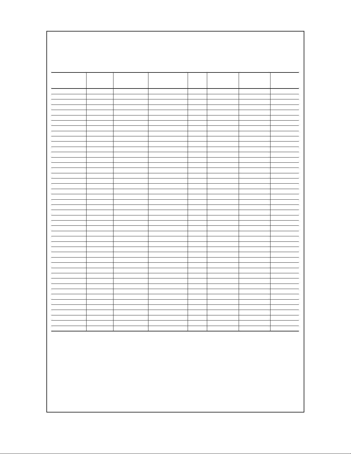
SMCJ5.0(C)A - SMCJ170(C)A
Electrical Characteristics T
Uni-directional
Bi-directional (C)
Device
Part
Marking*
Reverse
Stand-off Voltage
V
(V)
RWM
= 25°C unless otherwise noted
A
Breakdown Voltage
V
min max
BR
(V)
Test
Current
(mA)
IT
Max Clamping
Voltage @IPPM
VC (V)
Max Peak Pulse
Surge Current
I
(A)
PPM
Max Reverse
Leakage V
IR (uA)**
SMCJ5.0(C)A GDE 5.0 6.40 7.0 10 9.2 163.0 1000
SMCJ6.0(C)A GDG 6.0 6.67 7.37 10 10.3 145.6 1000
SMCJ6.5(C)A GDK(BDK) 6.5 7.22 7.98 10 11.2 133.9 500
SMCJ7.0(C)A GDM 7.0 7.78 8.60 10 12.0 125.0 200
SMCJ7.5(C)A GDP(BDP) 7.5 8.33 9.21 1 12.9 116.3 100
SMCJ8.0(C)A GDR(BDR) 8.0 8.89 9.83 1 13.6 110.3 50
SMCJ8.5(C)A GDT(BDT) 8.5 9.44 10.4 1 14.4 104.2 20
SMCJ9.0(C)A GDV(BDV) 9.0 10.0 11.1 1 15.4 97.4 10
SMCJ10(C)A GDX(BDX) 10 11.1 12.3 1 17.0 88.2 5
SMCJ11(C)A GDZ 11 12.2 13.5 1 18.2 82.4 5
SMCJ12(C)A GEE(BEE) 12 13.3 14.7 1 19.9 75.3 5
SMCJ13(C)A GEG 13 14.4 15.9 1 21.5 69.8 5
SMCJ14(C)A GEK(BEK) 14 15.6 17.2 1 23.2 64.7 5
SMCJ15(C)A GEM(BEM) 15 16.7 18.5 1 24.4 61.5 5
SMCJ16(C)A GEP 16 17.8 19.7 1 26.0 57.7 5
SMCJ17(C)A GER 17 18.9 20.9 1 27.6 54.3 5
SMCJ18(C)A GET(BET) 18 20.0 22.1 1 29.2 51.4 5
SMCJ20(C)A GEV(BEV) 20 22.2 24.5 1 32.4 46.3 5
SMCJ22(C)A GEX(BEX) 22 24.4 26.9 1 35.5 42.3 5
SMCJ24(C)A GEZ(BEZ) 24 26.7 29.5 1 38.9 38.6 5
SMCJ26(C)A GFE(BFE) 26 28.9 31.9 1 42.1 35.6 5
SMCJ28(C)A GFG(BFG) 28 31.1 34.4 1 45.4 33.0 5
SMCJ30(C)A GFK(BFK) 30 33.3 36.8 1 48.4 31.0 5
SMCJ33(C)A GFM(BFM) 33 36.7 40.6 1 53.3 28.1 5
SMCJ36(C)A GFP (BFP) 36 40.0 44.2 1 58.1 25.8 5
SMCJ40(C)A GFR(BFR) 40 44.4 49.1 1 64.5 23.3 5
SMCJ43(C)A GFT(BFT) 43 47.8 52.8 1 69.4 21.6 5
SMCJ45(C)A GFV 45 50.0 55.3 1 72.7 20.6 5
SMCJ48(C)A GFX 48 53.3 58.9 1 77.4 19.4 5
SMCJ51(C)A GFZ 51 56.7 62.7 1 82.4 18.2 5
SMCJ54(C)A GGE 54 60.0 66.3 1 87.1 17.2 5
SMCJ58(C)A GGG 58 64.4 71.2 1 93.6 16.0 5
SMCJ60(C)A GGK 60 66.7 73.7 1 96.8 15.5 5
SMCJ64(C)A GGM 64 71.1 78.6 1 103.0 14.6 5
SMCJ70(C)A GGP 70 77.8 86.0 1 113.0 13.3 5
SMCJ75(C)A GGR 75 83.3 92.1 1 121.0 12.4 5
SMCJ78(C)A GGT 78 86.7 95.8 1 126.0 11.9 5
SMCJ85(C)A GGV 85 94.4 104.0 1 137.0 10.9 5
SMCJ90(C)A GGX 90 100.0 111.1 1 146.0 10.3 5
SMCJ100(C)A GGZ 100 111.0 123.0 1 162.0 9.3 5
SMCJ110(C)A GHE 110 122.0 135.0 1 177.0 8.5 5
SMCJ120(C)A GHG 120 133.0 147.0 1 193.0 7.8 5
SMCJ130(C)A GHK 130 144.0 159.0 1 209.0 7.2 5
SMCJ150(C)A GHM 150 167.0 185.0 1 243.0 6.2 5
SMCJ160(C)A GHP 160 178.0 197.0 1 259.0 5.8 5
SMCJ170(C)A GHR 170 189.0 209.0 1 275.0 5.5 5
RWM
* Color band denotes cathode on unidirectional devices only. No color band on bidirectional
devices.
** For bidirectional parts with V
<10V, the IR max limit is doubled.
RWM
SMCJ5.0(C)A-SMCJ170(C)A, Rev. C
Page 3
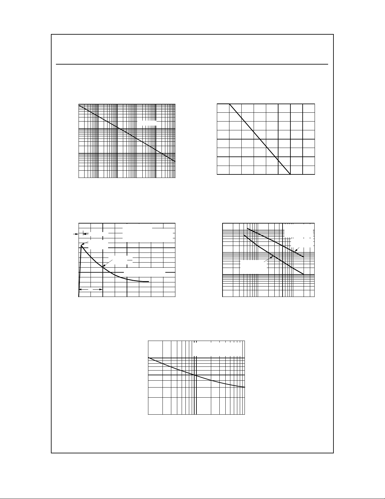
T ypical Characteristics
SMCJ5.0(C)A - SMCJ170(C)A
Transient Voltage Supressors
(continued)
Peak Pu l se Power Rati n g Cur v e
100
T = 25 C
º
A
10
1
PULSE POWER (kW)
0.1
0.0001 0.001 0.01 0.1 1 10
PULSE WIDTH (ms)
Pulse Waveform
150
µµµµ
tf = 10
sec
Peak Value
100
Ippm
50
PEAK PULSE CURRENT (%)
td
0
01234
T = 25 C
º
A
Pulse Width (td) is Defined
as the Point W h ere the Peak
Current Decays to 50% of Ipp
Half Value-Ipp
2
µµµµ
10/100 0
sec Waveform
as Defined by R.E.A.
e-kt
TIME (ms)
Pulse Derating Curve
100
75
50
PULSE P OWER (% )
25
0
0 25 50 75 100 125 150 175 200
AMBI ENT TEMPERATURE ( C)
º
Junction Capacitance
20000
10000
1000
Measured at
Stand-Off
100
CAPACITANCE (pF)
10
Voltage (V mw)
1 5 10 50 100 200 400
REVE RSE VOLTA GE (V)
T = 25 C
A
f = 1.0 MHz
Visg = 50m Vp-p
Measured a t
Zero Bias
º
Non-Repetitive Surge Current
200
100
50
20
FORWARD SURGE CURRENT (A)
10
12 51020 50100
NUMB ER OF CYCLES AT 60 Hz
T = T max
A
A
8.3ms Single Ha lf Sin e-Wave
JEDEC Method
SMCJ5.0(C)A-SMCJ170(C)A, Rev. C
Page 4

DO-214AB(SMC) Tape and Reel Data
DO-214AB(SMC) Packaging
Configuration: Figure 1.0
DO-214AB(SMC) Packaging Information
Packaging Option
Packaging type
Qty per Reel/Tube/Bag
Reel Size (inch diameter)
Box Dimension (mm)
Max qty per Box
Weight per unit (gm)
Weight per Reel (kg)
Note/Comments
Under package
code P5
TNR
3,000
13
336x336x38
6,000
0.210
1.130
Human readable label
Under package
code MA
TNR
3,000
13
336X336X38
6,000
0.210
1.130
Barcode label
Antistatic Cover Tape
Embossed Carrier Tape
Human
Readable/
Barcode
Label
F
B34
924
DO-214AB(SMC) unit orientation
336mm x 336mm x 38mm
Intermediate container for 13" reel option
Packaging Description:
DO-214AB(SMC) parts are shipped in tape. The carrier
tape is made from a dissipative (carbon filled)
polycarbonate resin. Alternate carrier tape is made of antistatic plastic. The cover tape is a multilayer film (Heat
Activated Adhesive in nature) primarily composed of
polyester film, adhesive layer, sealant, and anti-static
sprayed agent. These reeled parts in standard option are
shipped with 7,500 units per 13" or 330cm diameter reel.
The reel comes in plastic or carton which is made of
polystyrene plastic (anti-static coated) and thick white
paper respectively. Further information is described in the
Packaging Information table.
These full reels are individually labeled and placed inside
a bleach box (illustrated in figure 1.0) made of recyclable
carton paper with a Fairchild logo printing. One box
contains two reels maximum. Certain number of these
boxes are placed inside shipping box which comes in
different sizes depending on the number of parts shipped.
B34
F
924
B34
F
924
B34
F
924
Human
Readable/Barcode
Label (on top)
B34
Cathode
F
924
Human Readable Label sample
CAUTION: This container provides protection f or static sensitive devices. Handle devices with caution upon removal.
MADE IN ONE OR MORE OF THE FOLLOWING COUNTRIES: PHILIPPINES (MACTAN,
EXPORT PROCESSING ZONE), MALAYSIA, CHINA, S. KOREA, TAIWAN, THAILAND ,
SINGAPORE AND JAPAN.
3000
I.D
.
MBRS340
ANTI-STATIC
T0012 CBVK741B019
D/C
Qty
Lot
DO-214AB(SMC) Tape Leader and Trailer
Configuration: Figure 2.0
Carrier Tape
Cover Tape
Trailer Tape
160mm minimum or
Human readable/barcode Label
F63TNR Label sample
LOT: CBVK741B019
FSID: MBRS340
D/C1: T0012 QTY1: SPEC REV:
D/C2: QTY2: CPN:
FAIRCHILD SEMICONDUCTOR INTERNATIONAL
Components
QTY: 3000
SPEC:
(F63TNR)3.2
Leader Tape
390mm minimum
July 2000, Rev. A©2000 Fairchild Semiconductor International
Page 5

DO-214AB(SMC) Tape and Reel Data, continued
DO-214AB(SMC) Embossed Carrier Tape
Configuration: Figure 3.0
T
K0
Wc
B0
P0
D0
E1
F
W
E2
Tc
A0
P1
D1
User Direction of Feed
Dimensions are in millimeter
Pkgtype
DO-214AB(SMC)
(12mm)
Notes: A0, B0, and K0 dimensions are determined with respect to the EIA/Jedec RS-481
rotational and lateral movement requirements (see sketches A, B,and C).
A0 B0 W D0 D1 E1 E2 F P1 P0 K0 T Wc Tc
6.00
8.25
16.0
1.55
1.125
1.75
10.25
+/-0.15
+/-0.20
20 deg maximum component rotation
Sketch A (Side or Front Sectional View)
Component Rotation
+/-0.3
+/-0.05
+/-0.125
+/-0.10
B0
Sketch B (Top View)
Component Rotation
min
7.5
+/-0.05
20 deg maximum
A0
DO-214AB(SMC) Reel Configuration:
Figure 4.0
W1 Measured at Hub
8.0
+/-0.1
Typical
component
cavity
center line
Typical
component
center line
4.0
+/-0.1
2.4
0.40
+/-0.10
13.0
+/-0.3
0.5mm
maximum
+/-0.30
0.5mm
maximum
Sketch C (Top View)
Component lateral mov ement
B Min
Dim C
0.06
+/-0.02
Dim A
max
Tape Size
12mm 13" Dia
13" Diameter Option
Dimensions are in inches and millimeters
Reel
Option
Dim A Dim B Dim C Dim D Dim N Dim W1 Dim W2
13.0
0.059
330
1.5
Dim N
See detail AA
W2 max Measured at Hub
512 +0.020/-0.008
13 +0.5/-0.2
0.795
20.2
1.97
50 min
Dim D
min
0.646 +0.078/-0.000
16.4 +2/-0
DETAIL AA
0.724
18.4
July 2000, Rev. A
Page 6

DO-214AB(SMC) Package Dimensions
DO-214AB(SMC) (FS PKG Code P7)
1:1
Scale 1:1 on letter size paper
Dimensions shown below are in:
inches [millimeters]
Part Weight per unit (gram): 0.21
0.128 (3.25)
0.108 (2.743)
0.060 (1.524)
0.030 (0.762)
0.280 (7.112)
0.260 (6.604)
3.27
3.07
Minim um Recommended
2
0.320 (8.128)
0.305 (7.747)
0.008 (0.203)
0.002 (0.51)
1
0.245 (6.223)
0.220 (5.588)
0.103 (2.616)
0.079 (2.007)
0.012 (0.305)
0.006 (0.152)
6.18
5.98
+
4.69
4.49
7.67
7.47
Land Pattern
©2000 Fairchild Semiconductor International
August 1999, Rev . A
Page 7

TRADEMARKS
The following are registered and unregistered trademarks Fairchild Semiconductor owns or is authorized to use and is
not intended to be an exhaustive list of all such trademarks.
ACEx™
Bottomless™
CoolFET™
CROSSVOL T™
DenseTrench™
DOME™
EcoSPARK™
E2CMOS
EnSigna
TM
TM
FACT™
FACT Quiet Series™
FAST
FASTr™
GlobalOptoisolator™
GTO™
HiSeC™
ISOPLANAR™
LittleFET™
MicroFET™
MICROWIRE™
OPTOLOGIC™
OPTOPLANAR™
PACMAN™
POP™
PowerTrench
QFET™
QS™
QT Optoelectronics™
Quiet Series™
SILENT SWITCHER
SMART ST ART™
St ar* Power™
Stealth™
SuperSOT™-3
SuperSOT™-6
SuperSOT™-8
SyncFET™
TinyLogic™
UHC™
UltraFET
VCX™
DISCLAIMER
FAIRCHILD SEMICONDUCTOR RESERVES THE RIGHT TO MAKE CHANGES WITHOUT FURTHER
NOTICE TO ANY PRODUCTS HEREIN T O IMPROVE RELIABILITY , FUNCTION OR DESIGN. FAIRCHILD
DOES NOT ASSUME ANY LIABILITY ARISING OUT OF THE APPLICA TION OR USE OF ANY PRODUCT
OR CIRCUIT DESCRIBED HEREIN; NEITHER DOES IT CONVEY ANY LICENSE UNDER ITS PATENT
RIGHTS, NOR THE RIGHTS OF OTHERS.
LIFE SUPPORT POLICY
FAIRCHILD’S PRODUCTS ARE NOT AUTHORIZED FOR USE AS CRITICAL COMPONENTS IN LIFE SUPPORT
DEVICES OR SYSTEMS WITHOUT THE EXPRESS WRITTEN APPROVAL OF FAIRCHILD SEMICONDUCTOR CORPORA TION.
As used herein:
1. Life support devices or systems are devices or
systems which, (a) are intended for surgical implant into
the body, or (b) support or sustain life, or (c) whose
failure to perform when properly used in accordance
with instructions for use provided in the labeling, can be
reasonably expected to result in significant injury to the
user.
2. A critical component is any component of a life
support device or system whose failure to perform can
be reasonably expected to cause the failure of the life
support device or system, or to affect its safety or
effectiveness.
PRODUCT STA TUS DEFINITIONS
Definition of Terms
Datasheet Identification Product Status Definition
Advance Information
Preliminary
No Identification Needed
Obsolete
Formative or
In Design
First Production
Full Production
Not In Production
This datasheet contains the design specifications for
product development. Specifications may change in
any manner without notice.
This datasheet contains preliminary data, and
supplementary data will be published at a later date.
Fairchild Semiconductor reserves the right to make
changes at any time without notice in order to improve
design.
This datasheet contains final specifications. Fairchild
Semiconductor reserves the right to make changes at
any time without notice in order to improve design.
This datasheet contains specifications on a product
that has been discontinued by Fairchild semiconductor.
The datasheet is printed for reference information only.
Rev. H1
 Loading...