Fairchild SLTS218B service manual

查询PT78ST114供应商
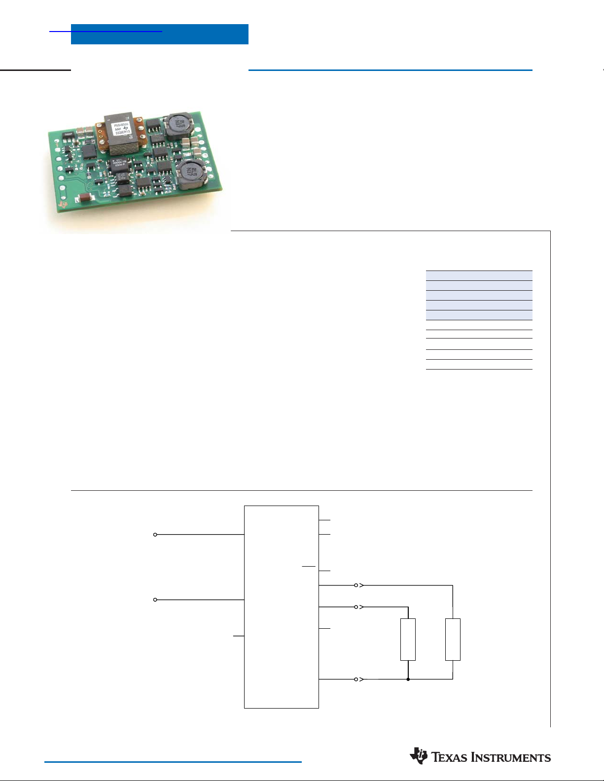
PTB48500, PTB48501, PTB48502
Dual-Output, 48-V Input Isolated
DC/DC Converter for xDSL
Description
The PTB4850x power modules are a
dual-output isolated DC/DC converter,
designed to provide the logic supply voltages for AC-7 based xDSL applications.
The PTB48500 is rated for 13 A of total
output current, making it suitable for
32-channel xDSL applications. The
PTB48501 and PTB48502 provide output
current for powering up to 64 xDSL channels. The PTB48501 is rated for 16.5 A
total output current, and the PTB48502,
21 A. The PTB48502 incorporates 10 W
of additional capacity for powering peripheral circuitry. Any of these converters can
be used for other applications with similar power requirements.
The modules operate from a standard
telecom (-48 V) central office (CO) supply
and include an “on/off” enable control,
SLTS218B - SEPTEMBER 2003 - REVISED NOVEMBER 2004
Features
• Dual Outputs
(Independently Regulated)
• Input Voltage Range:
36 V to 75 V
• Power-up/Down Sequencing
• 1500 VDC Isolation
• Over-Current Protection
• Over-Temperature Shutdown
• Under-Voltage Lockout
output current limit, over-temperature
protection, input under-voltage lockout
(UVLO). The PTB48500 and PTB48501
also incorporates a power-up reset (POR)
output.
The modules are designed to operate
with one of the PTB4851x DC/DC converter modules. The combination of a
PTB4850x and PTB4851x converter
provides the complete the power supply
for an AC7 chipset. The “EN Out” and
“Sync Out” pins provide compatible output signals for controlling both the power
up sequence and switching frequency of
the PTB48510.
The PTB4850x modules employ
double-sided surface mount construction,
and are an industry standard size.
• Fixed Frequency Operation
• Temp Range: –40 to 100 °C
• Industry Standard Outline
• Operates with PTB4851x for
Complete AC7 Power Solution
• Powers up to 64 DSL Ports
• Safety Approvals:
UL/cUL 60950
EN 60950
Pin Configuration
Pin Function
1+V
I
2 Sync Out
3 Enable #
4 EN Out
5–V
I
6+VO 2
7 COM
8 POR* / COM †
9Vo2 Adjust
10 +VO 1
Shaded functions indicate signals
that are referenced to –VI.
# Denotes positive logic:
Open = Normal operation
–V
= Outputs Off
I
* Denotes negative logic:
High = Normal operation
Low = Reset
† This pin is COM on the PTB48502
Stand-Alone Application
+V
I
–V
I
For technical support and further information visit http://power.ti.com
1
5
3
+V
–V
Enable
Sync Out
I
PTB4850x
I
EN Out
POR
Vo
Vo
Vo
Adj
2
COM
1
2
2
4
* Pin 8 is ‘COM’ on PTB48502
(8) *
Vo
Vo
COM
1
2
10
6
9
7, (8) *
L
O
A
D
L
O
A
D

PTB48500, PTB48501, PTB48502
Dual-Output, 48-V Input Isolated
DC/DC Converter for xDSL
Ordering Information
Base Part No. (PTB4850❒xxx)
Order Prefix Description
PTB48500xxx 13 A (32-Ports)
PTB48501xxx 16.5 A (48/64-Ports)
PTB48502xx 21 A (64-Ports + 10 W)
Notes: (1) Reference the applicable package reference drawing for the dimensions and PC board layout
(2) “Standard” option specifies 63/37, Sn/Pb pin solder material.
Output Voltage
Code Voltage
A 3.3 V / 1.2 V
(PTB4850x❒xx)
Pin Descriptions
+VI: The positive input supply for the module with respect
. When powering the module from a –48 V telecom
to –V
in
central office supply, this input is connected to the primary
system ground.
–V
: The negative input supply for the module, and the
I
0 VDC reference for the ‘Enable’, ‘EN Out’, and ‘Sync
Out’ signals. When the module is powered from a +48-V
supply, this input is connected to the 48-V Return.
V
1: The higher regulated power output voltage, which
O
is referenced to the COM node.
V
2: The lower regulated power output voltage, which
0
is referenced to the COM node.
COM: The secondary return reference for the module’s two
regulated output voltages. It is dc isolated from the input
supply pins.
V
2 Adjust: Using a single resistor, this pin allows Vo2 to
O
be adjusted higher or lower than the preset value. If not
used, this pin should be left open circuit.
Enable: This is an open-collector (open-drain) positive
logic input that enables the module output. This pin is
referenced to -Vin. A logic ‘0’ at this pin disables the
module’s outputs, and a high impedance enables the outputs. If not used the pin should be left unconnected.
EN Out: This open-collector output may be used to enable
the output of other DC/DC converters in applications
where the power-up sequence of the related voltages must
be precisely controlled. The output is used principally to
control the startup up of a PTB4851xx module when
powering ADSL circuits based on the AC7 chipset. The
signal is referenced to -Vin, and is active low. It is initially
‘off’ (high impedance), and turns ‘on’ when the output
voltage, Vo
Sync Out: The signal generated by this pin is designed to
be used exclusively with the PTB48510 in AC7 ADSL
applications. When the ‘Sync Out’ of this converter is
connected directly to the ‘Sync In’ pin of the PTB48510,
both modules will operate at the same switch conversion
frequency.
POR*: (Available to PTB48500 and PTB48501 only!)
This pin produces an active-low power-on reset signal
that may be used to reset logic circuitry. The output is
set low during power up just as the output voltage from
Vo
starts to rise. It remains low for 10 ms after the volt-
1
age at Vo1 has reached its nominal set-point voltage.
This signal is referenced to the COM node, and has a
3.3-kΩ internal pull-up resistor to Vo
SLTS218B - SEPTEMBER 2003 - REVISED NOVEMBER 2004
Package Options
Code Description Pkg Ref.
AH Horiz. T/H (ERH)
AS SMD, Standard
, has risen to its nominal set-point voltage.
1
(PT4850xx❒❒)
(2)
1
(ERJ)
.
(1)
Environmental and General Specifications (Unless otherwise stated, all voltages are with respect to –V
Characteristics Symbols Conditions Min Typ Max Units
Input Voltage Range V
Isolation Voltage Input–output/input–case 1500 — — V
Capacitance Input to output — 1500 — pF
Resistance Input to output 10 — — MΩ
Operating Temperature Range T
Over-Temperature Protection OTP Shutdown threshold — 115 —
Solder Reflow Temperature T
Storage Temperature T
Mechanical Shock Per Mil-STD-883D, Method 2002.3
Mechanical Vibration Mil-STD-883D, Method 2007.2 Suffix H — 20 —
Weight — — 20 — grams
Flammability — Meets UL 94V-O
Notes: (i) During reflow of SMD package version do not elevate peak temperature of the module, pins or internal components above the stated maximum.
in
a
reflow
s
Over output load range 36 48 75 VDC
Over Vin Range –40 — +85 °C
Hysterisis — 10 —
Surface temperature of module body or pins 235
— –40 — 125 °C
1 msec, ½ Sine, mounted
20-2000 Hz Suffix C — 5 —
— 500 — G’s
For technical support and further information visit http://power.ti.com
)
in
(i)
°C
°C
G’s

PTB48500
Dual-Output, 48-V Input Isolated
DC/DC Converter for xDSL
Specifications (Unless otherwise stated, T
=25°C, VI =48 V, CI =0µF, CO =0 µF, and IO =50% Iomax)
A
SLTS218B - SEPTEMBER 2003 - REVISED NOVEMBER 2004
PTB48500A
Characteristic Symbol Conditions Min Typ Max Units
Output Power Po
Output Current Io
Output Voltage Vo
Temperature Variation ∆Reg
Line Regulation ∆Reg
Load Regulation ∆Reg
Cross Regulation ∆Reg
Efficiency η Io
Vo Ripple (pk-pk) V
Transient Response t
Over Current Threshold Iotrip VI =36 V,
, Po
1
Po
total
, Io
1
Io1 + Io
1
Vo
2
r
tr
∆V
tr
temp
line
load
cross
2
Both outputs — — 28 W
2
Over VI range Vo1 (3.3 V) 0 — 6
Total (both outputs) 0 — 13 A
2
Inlcudes set point, line, load, 3.2 3.3 3.4
–40 ≤ TA ≤ +85°C 1.16 1.2 1.24
–40° ≤TA ≤ +85°C, I
Over VI range Vo1, Vo
Over IO range Vo1, Vo
I
min ≤ Io2 ≤ I
O
I
min ≤ Io1 ≤ I
O
, Io2 =Iomax — 82 — %
1
20 MHz bandwidth Vo
1 A/µs load step, 50% to 100% Iomax — 30 — µs
Vo1, Vo2 over/undershoot — ±2.0 — %V
reset followed by auto-recovery
=IO min Vo
O
max, Io
=1 A ∆Vo
o
1
max, Io
=1 A ∆Vo
o
2
Vo1 (3.3 V) — — 19.8
Vo2 (1.2 V) — — 8.4
Vo2 (1.2 V) 0 — 7
— ±0.5 —
1
Vo
— ±0.8 —
2
— ±1 ±10 mV
2
— ±3 ±12 mV
2
——10
1
——10
2
—2050
1
Vo
—2050
2
Io
1
+ Io
13.5 16 — A
2
(1)
(1)
Output Voltage Adjust Range Vadj Vo2 only -10 — +20 %V
Switching Frequency ƒ
Under-Voltage Lockout VI on VI increasing — 34 —
On/Off Enable (pin 3) Referenced to –VI (pin 5)
Input High Voltage V
Input Low Voltage V
Input Low Current I
s
VI off VI decreasing — 32 —
IH
IL
IL
Over VI and IO ranges 500 550 600 kHz
+3.6 — +75
–0.2 — +0.8
(2)
—–1—mA
Standby Input Current II standby pins 3 & 5 connected — 2 — mA
Internal Input Capacitance C
External Output Capacitance Co
Reliability MTBF Per Telcordia SR-332
Notes: (1) See Safe Operating Area curves or contact the factory for the appropriate derating.
(2) The On/Off Enable (pin 3) has an internal pull-up and may be controlled with an open-collector (or open-drain) transistor. The input is diode protected
and may be connected to +VI. The maximum open-circuit voltage is 7 V. If it is left open circuit the converter will operate when input power is applied.
Co
I
1
2
50% stress, TA =40°C, ground benign
—2 —µF
(3)
0
0
(3)
— 5,000
— 5,000
1.5 — — 10
(3) An output capacitor is not required.
W
A
V
%V
mV
mV
V
V
µF
6
o
pp
o
o
Hrs
For technical support and further information visit http://power.ti.com

PTB48500
Typical Characteristics
Dual-Output, 48-V Input Isolated
DC/DC Converter for xDSL
PTB48500A Characteristic Data (See Note A)
Efficiency vs Load Current (See Note B)
100
90
80
70
Efficiency - %
60
50
024681012
Power Dissipation vs Load Current (See Note B)
10
8
6
4
Pd - Watts
Io1 + Io2 (A)
SLTS218B - SEPTEMBER 2003 - REVISED NOVEMBER 2004
Safe Operating Area PTB48500A (See Note C)
V
=48 VDC (See Note B)
IN
90
80
V
IN
48 V
36 V
75 V
V
IN
48 V
36 V
75 V
70
60
50
40
Ambient Temperature (°C)
30
20
0 5 10 15 20 25 30
Total Output Power (W)
Airflow
400LFM
200LFM
100LFM
Nat Conv
2
0
024681012
Cross Regulation,
6
4
(mV)
o
2
0
-2
Cross Regulation ∆V
-4
-6
01234567
Io1 + Io2 (A)
∆∆
∆Vo
vs Ioy @Iox =1 A & VIN =48 V
∆∆
x
Io1 : Io2 (A)
Vo1 vs Io
Vo2 vs Io
2
1
Note A: Characteristic data has been developed from actual products tested at 25°C. This data is considered typical data for the converter.
Note B: Load current is increased proportionally from both outputs, up to the respective maximum value of each output.
Note C: SOA curves represent the conditions at which internal components are at or below the manufacturer’s maximum operating temperatures. Derating limits apply to
modules soldered directly to a 4 in. × 4 in. double-sided PCB with 1 oz. copper.
For technical support and further information visit http://power.ti.com

PTB48501
Dual-Output, 48-V Input Isolated
DC/DC Converter for xDSL
Specifications (Unless otherwise stated, T
=25°C, VI =48 V, CI =0 µF, CO =0 µF, and Io =50% IO max)
A
SLTS218B - SEPTEMBER 2003 - REVISED NOVEMBER 2004
PTB48501A
Characteristic Symbol Conditions Min Typ Max Units
Output Power Po
Output Current Io1, Io
Output Voltage Vo
Temperature Variation ∆Reg
Line Regulation ∆Reg
Load Regulation ∆Reg
Cross Regulation ∆Reg
Efficiency η Io
Vo Ripple (pk-pk) V
Transient Response t
Over Current Threshold IO trip VI =36V,
, Po
1
Po
total
Io1 + Io
1
Vo
2
r
tr
∆V
tr
temp
line
load
cross
2
Both outputs — — 32.4 W
2
Over VI range Vo1 (3.3 V) 0 — 6
Total (both outputs) 0 — 16.5 A
2
Inlcudes set point, line, load, 3.2 3.3 3.4
–40 ≤ TA ≤ +85°C 1.16 1.2 1.24
–40° ≤TA ≤ +85°C, I
Over VI range Vo1, Vo
Over Io range Vo1, Vo
I
min ≤ Io2 ≤ I
O
I
min ≤ Io1 ≤ I
O
, Io2 =Iomax — 81 — %
1
20 MHz bandwidth Vo
1 A/µs load step, 50% to 100% Iomax — 30 — µs
Vo1, Vo2 over/undershoot — ±2.0 — %V
reset followed by auto-recovery
=IO min Vo
O
max, Io
=1 A ∆Vo
o
1
max, Io
=1 A ∆Vo
o
2
Vo1 (3.3 V) — — 19.8
Vo2 (1.2 V) — — 12.6
(1)
Vo2 (1.2 V) 0 — 10.5
— ±0.5 —
1
Vo
— ±0.8 —
2
— ±1 ±10 mV
2
— ±3 ±12 mV
2
——10
1
——10
2
—2050
1
Vo
—2050
2
Io
1
+ Io
—24—A
2
(1)
Output Voltage Adjust Range Vadj Vo2 only –20 — +10 %V
Switching Frequency ƒ
Under-Voltage Lockout V
On/Off Enable (pin 3) Referenced to –VI (pin 5)
Input High Voltage V
Input Low Voltage V
Input Low Current I
s
on VI increasing — 34 —
I
VI off VI decreasing — 32 —
IH
IL
IL —–1—mA
Over VI and IO ranges 500 550 600 kHz
+3.6 — +75
–0.2 — +0.8
(2)
Standby Input Current II standby pins 3 & 5 connected — 2 — mA
Internal Input Capacitance C
External Output Capacitance Co
Reliability MTBF Per Telcordia SR-332
Notes: (1) See Safe Operating Area curves or contact the factory for the appropriate derating.
(2) The On/Off Enable (pin 3) has an internal pull-up and may be controlled with an open-collector (or open-drain) transistor. The input is diode protected
and may be connected to +VI. The maximum open-circuit voltage is 7 V. If it is left open circuit the converter will operate when input power is applied.
Co
I
1
2
50% stress, TA =40°C, ground benign
—2 —µF
(3)
0
0
(3)
— 5,000
— 5,000
1.5 — — 10
(3) An output capacitor is not required.
W
A
V
%V
mV
mV
V
V
µF
6
o
pp
o
o
Hrs
For technical support and further information visit http://power.ti.com
 Loading...