Fairchild SI4542DY service manual

Si4542DY
30V Complementary PowerTrench
MOSFET
Si4542DY
January 2001
General Description
This complementary MOSFET device is produced using
Fairchild’s advanced PowerTrench process that has
been especially tailored to minimize the on-state
resistance and yet maintain low gate charge for
superior switching performance.
Applications
• DC/DC converter
• Power management
D2
D
D2
D
D1
D
D1
D
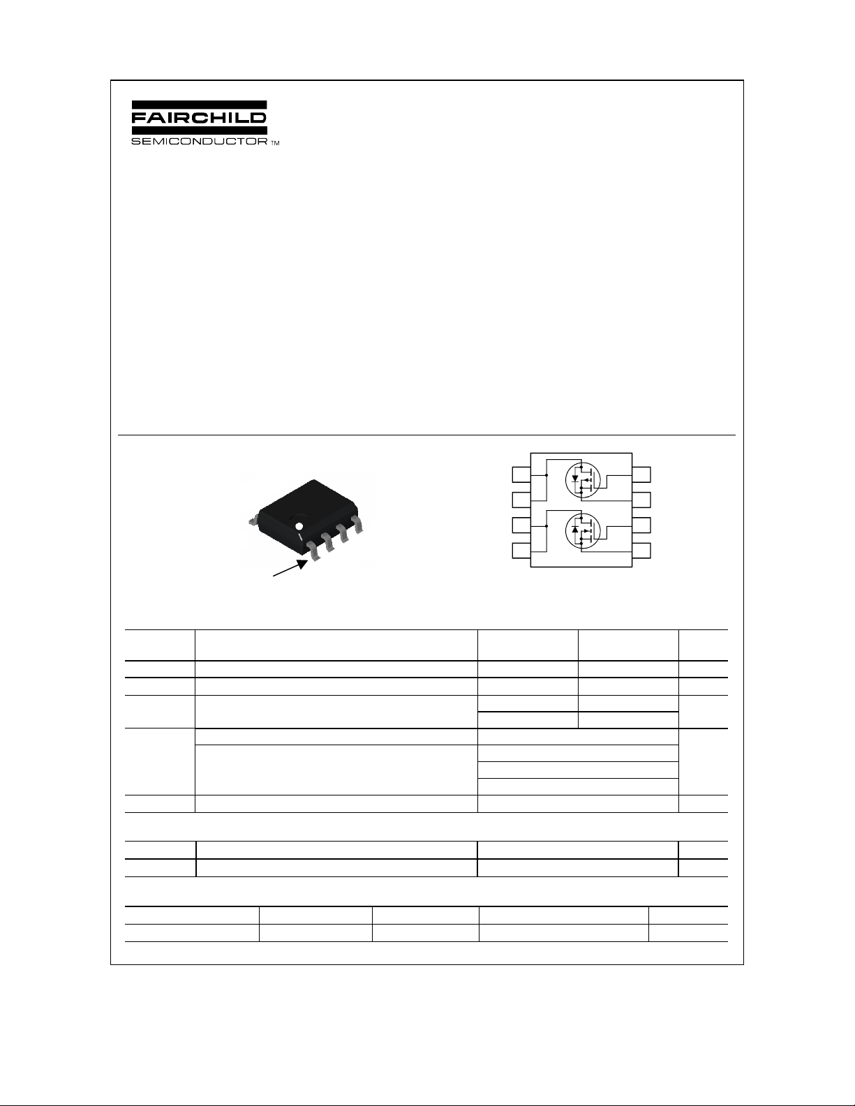
SO-8
Pin 1
SO-8
S1
Absolute Maximum Ratings T
G2
S2
G
G1
S
S
S
= 25°C unless otherwise noted
A
Features
• Q1: N-Channel
6 A, 30 V R
R
• Q2: P-Channel
–6 A, –30 V R
R
Q2
5
6
Q1
7
8
= 28 mΩ @ V
DS(on)
= 35 mΩ @ V
DS(on)
= 32 mΩ @ V
DS(on)
= 45 mΩ @ V
DS(on)
= 10V
GS
= 4.5V
GS
= –10V
GS
= –4.5V
GS
4
3
2
1
Symbol Parameter Q1 Q2 Units
V
DSS
V
GSS
I
D
P
D
TJ, T
STG
Drain-Source Voltage 30 –30 V
Gate-Source Voltage
±20 ±20
Drain Current - Continuous (Note 1a) 6–6A
- Pulsed 20 –20
Power Dissipation for Dual Operation 2 W
Power Dissipation for Single Operation (Note 1a) 1.6
(Note 1b)
(Note 1c)
1.2
1
Operating and Storage Junction Temperature Range –55 to +175
V
°C
Thermal Characteristics
R
θJA
R
θJC
Thermal Resistance, Junction-to-Ambient (Note 1a) 78
Thermal Resistance, Junction-to-Case (Note 1) 40
Package Marking and Ordering Information
Device Marking Device Reel Size Tape width Quantity
4542 Si4542DY 13” 12mm 2500 units
2001 Fairchild Semiconductor International
°C/W
°C/W
Si4542DY Rev A

Si4542DY
Electrical Characteristics T
= 25°C unless otherwise noted
A
Symbol Parameter Test Conditions Type Min Typ Max Units
Off Characteristics
BV
DSS
∆BVDSS
∆T
J
I
DSS
I
GSS
Drain-Source Breakdown
Voltage
Breakdown Voltage
Temperature Coefficient
Zero Gate Voltage Drain
Current
VGS = 0 V, ID = 250 µA
= 0 V, ID = –250 µA
V
GS
= 250 µA, Referenced to 25°C
I
D
= –250 µA, Referenced to 25°C
I
D
VDS = 24 V, VGS = 0 V
V
= –24 V, VGS = 0 V
DS
Gate-Body Leakage VGS = +20 V, VDS = 0 V
VGS = +20 V, VDS = 0 V
Q1
Q230–30
Q1
Q2
Q1
Q2
Q1
Q2
23
–21
+100
+100
–1
V
mV/°C
1
µA
nA
On Characteristics (Note 2)
V
GS(th)
∆VGS(th)
∆T
J
R
DS(on)
I
D(on)
g
FS
Gate Threshold Voltage VDS = VGS, ID = 250 µA
= VGS, ID = –250 µA
V
Gate Threshold Voltage
Temperature Coefficient
Static Drain-Source
On-Resistance
DS
I
= 250 µA, Referenced to 25°C
D
= –250 µA, Referenced to 25°C
I
D
VGS = 10 V, ID = 6 A
= 10 V, ID = 6 A, TJ = 125°C
V
GS
= 4.5 V, ID = 5 A
V
GS
VGS = –10 V, ID = –6 A
= –10 V, ID = –6 A, TJ = 125°C
V
GS
= –4.5 V, ID = –5 A
V
GS
On-State Drain Current VGS = 10 V, VDS = 5 V
V
= –10 V, VDS = –5 V
GS
Forward Transconductance VDS = 15 V, ID = 6 A
= –10 V, ID = –6 A
V
DS
Q1
Q2
Q1
Q2
Q1 19
Q2
Q1
Q220–20
Q1
Q2
1–11.5
–1.73–3
–4
32
25
21
29
30
18
16
V
mV/°C
4
28
mΩ
48
35
32
51
45
A
S
Dynamic C haracteristics
C
iss
C
oss
C
rss
Input Capacitance Q1
Output Capacitance Q1
Reverse Transfer
Capacitance
Q1
= 15 V, VGS = 0 V,
V
DS
f = 1.0 MHz
Q2
= –15 V, VGS = 0 V,
V
DS
f = 1.0 MHz
Q2
Q2
Q1
Q2
830
1540
185
400
80
170
pF
pF
pF
Electrical Characteristics (continued) T
= 25°C unless otherwise noted
A
Symbol Parameter Test Conditions Type Min Typ Max Units
Switching Characteristics (Note 2)
t
t
t
t
Q
Q
Q
d(on)
r
d(off)
f
g
gs
gd
Turn-On Delay Time Q1
Turn-On Rise Time Q1
Turn-Off Delay Time Q1
Turn-Off Fall Time
Total Gate Charge Q1
Gate-Source Charge Q1
Gate-Drain Charge
Q1
VDS = 15 V, ID = 1 A,
V
GS
= 10V, R
GEN
= 6 Ω
Q2
= –15 V, ID = –1 A,
V
DS
= –10 V, R
V
GS
GEN
= 6 Ω
Q1
V
= 15 V, ID = 7.5 A, VGS = 5 V
DS
Q2
V
= –10 V, ID = –6 A, VGS = –5V
DS
Q2
Q2
Q2
Q1
Q2
Q2
Q2
Q1
Q2
13
10
22
18
47
18
15
2.8
3.1
6
12
ns
24
18
ns
35
29
ns
75
5
12
ns
30
9
13
nC
20
nC
4
nC
5
Si4542DY Rev A
 Loading...