


www.fairchildsemi.com
AN-6902
Applying SG6902 to Control a CCM PFC and
Flyback/PWM Power Supply
Summary
This application note shows a step-by-step design to a
120W/24V power adapter. The equations also can be
applied to different output voltages and wattages.
Features
Interleaved PFC/PWM Switching
Green-Mode PFC/PWM Switching
No PFC Switching at Light Loads for Power Saving
Innovative Switching Charge Multiplier-divider
Low Startup and Operating Current
Innovative Switching Charge Multiplier-divider
Multi-vector Control for Improved PFC Output
Transient Response
Average-Current-Mode Control for PFC
Programmable Two-Level PFC Output Voltage to
Achieve the Best Efficiency
PFC Over-voltage and Under-voltage Protections
PFC and PWM Feedback Open-loop Protection
Cycle-by-cycle Current Limiting for PFC/PWM
Slope Compensation for PWM
Maximum Power Limit for PWM
Brownout Protection
Over Temperature Protection
Power-on Sequence Control and Soft-start
20-Pin SOP and SSOP Packages
Description
SG6902 is designed for power supplies that consist of boost
PFC and flyback PWM. It requires few external
components to achieve green-mode operation and versatile
protections and compensations.
The proprietary interleave switching synchronizes the PFC
and PWM stages and reduces switching noise. At light
loads, PFC stage is turned off to save power and the PWM
switching frequency is decreased in response to the load.
For PFC stage, the proprietary multi-vector control scheme
provides a fast transient response in a low-bandwidth PFC
loop. The overshoot and undershoot of the PFC voltage are
clamped. If the feedback loop is broken, SG6902 shuts off
the switching to protect the power supply and its load.
For the flyback PWM stage, the synchronized slope
compensation ensures the stability of the current loop.
“Hiccup” operation limits a maximum output power during
the overload situations.
The difference between members of this family are shown
in the table below.
Parameter SG6902 SG6901A
Start Threshold Voltage
Minimum Operating Voltage
The Interval of OPFC Lags
Behind OPWM at Startup
PFC On/Off
OTP
Soft-Start
16V 12V
10V 10V
11.5ms 11.5ms
O X
O O
O O
© 2007 Fairchild Semiconductor Corporation www.fairchildsemi.com
Rev. 1.2.1 • 5/1/08
AN-6902 APPLICATION NOTE
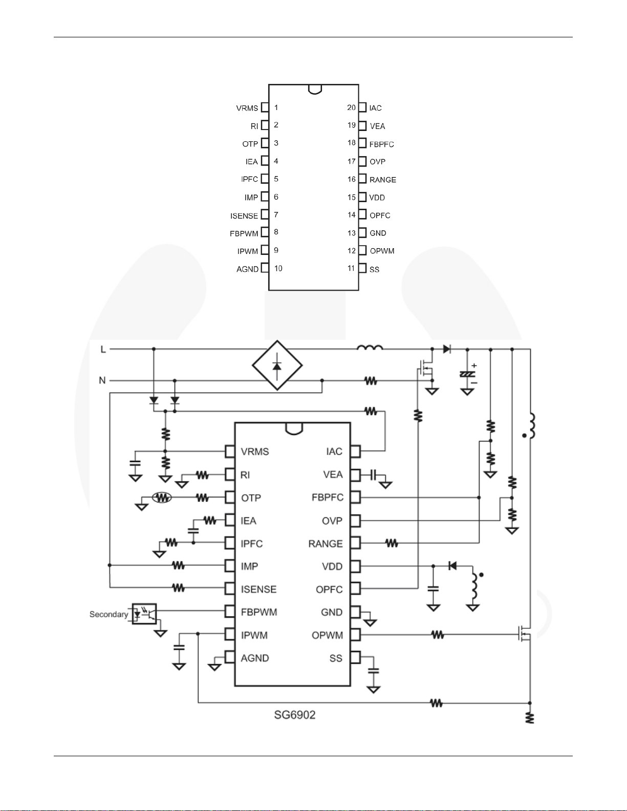
Pin Configuration
Figure 1. Pin Configuration
Typical Application
Figure 2. Typical Application
© 2007 Fairchild Semiconductor Corporation www.fairchildsemi.com
Rev. 1.2.1 • 5/1/08 2
AN-6902 APPLICATION NOTE
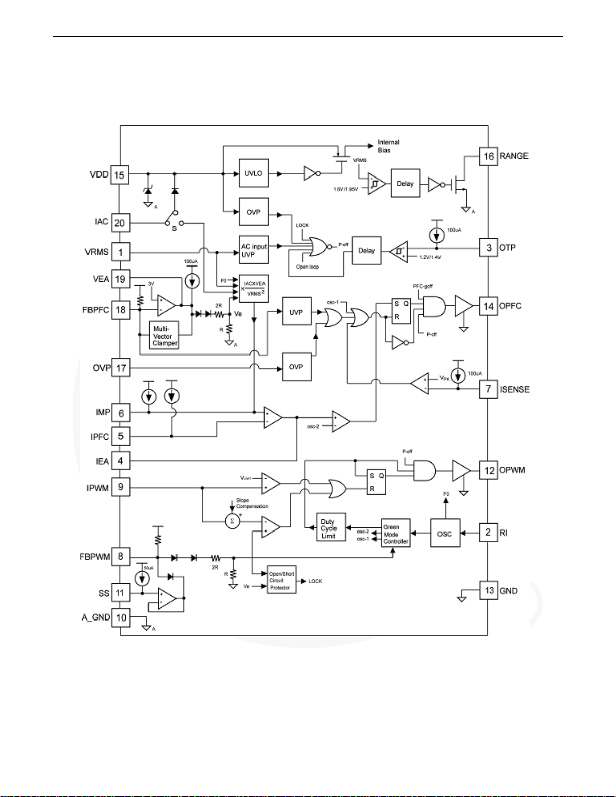
Block Diagram
Figure 3. Block Diagram
© 2007 Fairchild Semiconductor Corporation www.fairchildsemi.com
Rev. 1.2.1 • 5/1/08 3
AN-6902 APPLICATION NOTE
PFC Section
Power-On Sequence
Because the capacitor includes ±20% variation, the
capacitor 100µF is chosen.
SG6902 is active when the line voltage is higher than the
brownout threshold. The PWM stage is switching first,
then, following an 11.5ms delay time after FBPWM
voltage is higher than a PFC turn-on threshold voltage,
the PFC stage is enabled.
PFC Inductor
The switching frequency fS, output power P
efficiency n, maximum ripple current ΔI, and minimum
input voltage V
should be defined before determining
IN.min
the inductance of PFC inductor. The following equations
are utilized to determine the inductance of the PFC
inductor. Normally the maximum ripple current is 20% ~
30% of maximum input current.
()
OUT
I×=Δ
V
3.0/P2
η
)MIN(IN
1D×−=
V
O
2V
min.IN
di
LV =
dt
max
fs/D
IN.min
L
××=2V
I
Δ
For a 120W adapter power, η= 0.85, V
= 65KHz, VO = 250V, ΔI = 0.66A, D = 0.49, L =
f
S
IN(MIN)
= 90V
0.4mH.
PFC Capacitor
An advantage of using interleaving switching of PFC and
PWM stage is to reduce the switching noise. The ESR
requirement of boost capacitor is relaxed. The boost
capacitor value is chosen to remain a hold-up time of
output voltage in the event line voltage is removed.
××
=
C
O
()
η
where V
is the minimum output voltage in accordance
O.min
with the requirement of the specification.
For a 120W power supply, the capacitor is determined as:
C
© 2007 Fairchild Semiconductor Corporation www.fairchildsemi.com
Rev. 1.2.1 • 5/1/08 4
()
>
O
()
2
t)/(P2
up-holdPWMOUT
2
ripple)normal(O
ms1585.0/W1202
××
2
6020250
−−
2
VVV −−
min.O
F86
μ
=
(1)
(2)
(3)
(4)
AC,
(5)
(6)
OUT
,
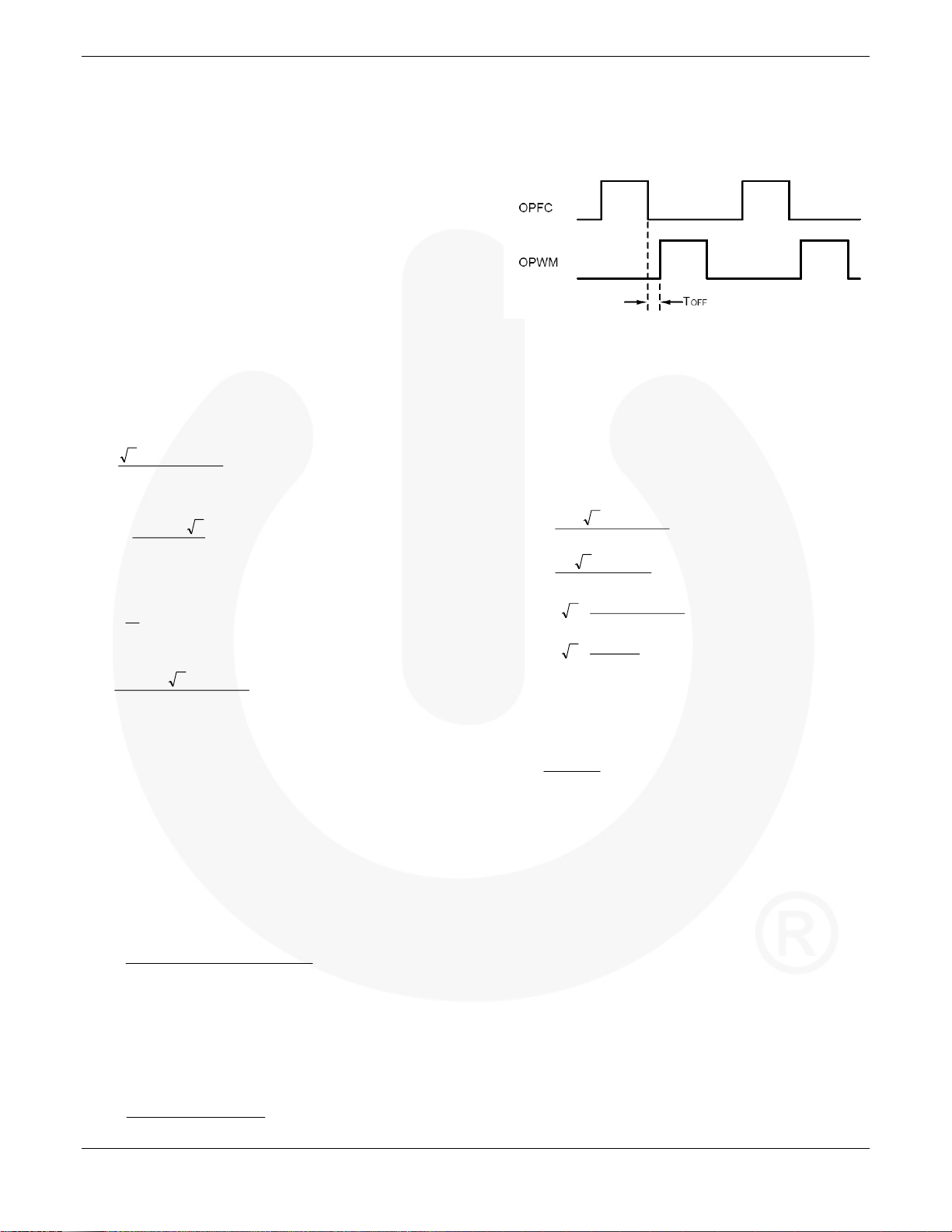
Figure 4. Interleaving Switching
Boost Rectifier and Switch
The fast reverse-recovery time of the boost diode is
required to reduce the power losses and the EMI. A 500V
voltage rating is chosen to withstand 400V boosts
potential. The average current and peak currents flow
through the boost diode and the switch, respectively, and
are given by:
η
/P22
××
I
AVG
I
AVG
PEAK
PEAK
=
π
×
=
2I
2I
OUT
V
××
π
75
×
×=
V
75
OUT
8.0/120
)Brownout(RMS
8.0/12022
A8.1
=
η
/P
)Brownout(RMS
A82.2
=×=
(7)
Oscillation and Green Mode
The resistor RI connected from the RI to GND pin
programs the switching frequency of SG6902.
1560
=
f
S
()
KR
Ω
I
For example, a 24kΩ resistor R
()
KHz
(8)
results in a 65kHz
I
switching frequency. The recommended range for the
switching frequency is 33kHz ~ 100kHz.
SG6902 provides an off-time modulation to reduce the
switching frequency in light-load and no-load conditions.
The feedback voltage of FBPWM pin is taken as
reference. When the feedback voltage is lower than about
2.1V, the switching frequency decreases accordingly.
Most of losses in a switching-mode power supply are
proportional to the switching frequency; therefore, the
off-time modulation reduces the power consumption of
the power supply in light-load and no-load conditions.
For a typical case of R
= 24KΩ, the switching frequency
I
is 65kHz at nominal load and decreases to 20kHz at light
load. The switching signal is disabled if the switching
frequency falls below 20KHz, which avoids acoustic noise.
For stability reasons, a capacitor connecting the RI pin to
GND is not suggested.

AN-6902 APPLICATION NOTE
f
F
s
20KHz
2.1
BPWM(V)
Figure 5. Switching Frequency vs. FB Voltage
To save power, the PFC stage is enabled only when the
feedback voltage of the FBPWM pin is higher than a
threshold voltage V
. The threshold voltage VTH is 2.1V
TH
to 2.45V at low line voltage input, 1.95V at high line
voltage. The threshold voltage V
determines an output
TH
power threshold to turn on/off the PFC stage for the
power saving. The output power P
can be expressed
OUT
as:
P
OUT
FB
where V
η
=
is a synchronized 0.5V ramp.
SL
ONIN
tL2
××
P
V
⎧
⎪
3V2.1V
⎨
⎪
⎩
)PEAK(IN
L
P
V
SL
tR
ONS
t
×+×××+=
t
ON
(9)
⎫
⎪
(10)
⎬
⎪
⎭
2
tV
××
()
Equation 10 shows that, through the feedback loop, the
on-time t
switching period t and/or the inductance L
changes in response to the change of the
ON
(the primary
P
inductance of the transformer) for providing a same
output power. Because the feedback voltage V
the on-time t
, a lower VFB causes a narrow on-time tON.
ON
controls
FB
Changing the switching frequency (the switching period
t) and the inductance L
, affects the output power
P
threshold to on/off the PFC stage.
IAC Signal
Figure 6 shows that the IAC pin is connected to the input
voltage via a resistor. A current I
multiplier.
I ≈
)PEAK(AC
V
)PEAK(IN
R
AC
For wide range input:
()
PEAKIN
=×=
is used for PFC
AC
V3742V264V
(11)
(12)
Figure 6. Linear Range
Line Voltage Detection (VRMS)
Figure 6 shows a resistive divider with low-pass filter
connected to the VRMS
The V
input is used for the PFC multiplier and
RMS
brownout protection.
For a sine wave input voltage, the voltage on the VRMS
pin is directly proportional to input voltage. To achieve
the brownout protection, the PFC stage is disabled after a
195ms delay once the V
The PWM stage is protected through the open-loop
detection on the FBPWM pin when the output voltage of
the PFC stage is too low. After that, SG6902 turns off.
When V
voltage is higher than 0.98V, the SG6902
RMS
restarts in accordance with power-on sequence of PFC
and PWM stages.
For example, a brownout protection is set as 75V
and RI can be determined as:
R
RMS
IN)MEAN(IN
V
RMS
=
1R
+
R1R
RMS
The threshold of V
V
= 75VAC, the value of R1 is 56.8KΩ.
IN
pin for line-voltage detection.
voltage drops below 0.8V.
RMS
2
2VV
××=
π
2
×××
2V
IN
= 0.8V. If R
RMS
π
= 4.8MΩ and
RMS
AC
. The
(13)
(14)
The linear range of I
suggested for a wide input range (90V
© 2007 Fairchild Semiconductor Corporation www.fairchildsemi.com
Rev. 1.2.1 • 5/1/08 5
is 0~360µA. A 1.2M resistor is
AC
~ 264VAC).
AC

AN-6902 APPLICATION NOTE
(
PFC Operation
Cycle-by-cycle Current Limiting
SG6902 provides cycle-by-cycle current limiting for both
PFC and PWM stages. Figure 8 shows the peak current
limit for the PFC stage. The switching signal of PFC
stage is turned off immediately once the voltage on
ISENSE pin goes below the threshold voltage V
The voltage of V
. The correlation of the threshold voltage VPK and
V
PK
determines the threshold voltage
RMS
PK
.
VRMS is shown in Figure 8. The amplitude of the
shown in Figure 8 is determined by a
P
, in accordance with the following
T
Figure 7. Current Output
constant current I
reference current I
equation as:
The current source output from the switching charge
multiplier/divider can be expressed as:
MO
V
RMS
EAAC
2
KI
×=
)A(
μ
(15)
VI
×
According to Figure 7, the current output from IMP pin,
, is the summation of IMO and I
I
MP
equipped as same as R
is identical with I
. The constant current source I
3
. They are used to bias (pull HIGH)
MR2
. The resistor R2 is
MR1
MR1
Tp
Therefore, the peak current of the I
I
=
PEAK_S
V2.1
2I2I ×=×=
R
I
can be expressed as:
S
)
V2.0RI
−×
PP
R
S
(19)
(20)
the operating point of the IMP and IPFC pins since the
voltage across R
goes negative with respect to ground.
S
Through the differential amplification of the signal across
, a better noise immunity is acjoeved. The output of IEA
R
S
compared with an internal sawtooth generates a switching
signal for PFC. Through the feedback loop of the average
current control mode, the input current I
:
to I
MO
RIRI ×=×
SS2MO
According to this equation, the minimum value of R
maximum value of R
can be determined. The IMO should
S
be estimated under its specified maximum value.
A concern in determining the value of the sense resistor
includes low-resistance RS reduces the power
R
S
consumption, but high-resistance R
resolution to achieve low input current THD (total
harmonic distortion). Using a current transformer (CT)
instead of R
improves the efficiency for high-power
S
converters.For a 120W adapter, the power consumption of
= 0.36Ω is:
R
S
2
85.0/W120
90
⎞
⎟
⎠
=×
⎛
P
=
⎜
RS
⎝
R
and R3 can be determined as
2
(the brownout threshold is 75V):
120W/0.8
I
I
MO
MO
MAX
75V
IR
×
MAXS
=
R
2
2.830.36
×
=
3.3K
The results show that R
308μ0
=
2.83A2
=×=I
, R2, and R3 values are fit for
S
providing 120W output.
© 2007 Fairchild Semiconductor Corporation www.fairchildsemi.com
Rev. 1.2.1 • 5/1/08 6
is proportional
S
provides high
S
W885.036.0
(16)
and
2
(17)
(18)
Figure 8. Current Limit
Multi-vector Error Amplifier
To achieve good power factor, the voltage for V
should be kept as DC-value according to Equation
V
EA
14. In other words, a low-pass RC filtering for V
narrow bandwidth (lower than the line frequency) of PFC
voltage loop are suggested to achieve better input current
shaping. The trans-conductance error amplifier has output
impedance R
(>90kΩ). A capacitor CEA (1µF ~ 10µF) is
O
suggested to connect from the output of the error
amplifier to ground (Figure 9). A dominant pole f
PFC voltage loop is shown as:
f××=
1
1
π
CR2
EAO
The average total input power can be expressed as:
IVP
×=
()()
IV
×∞
MORMS
V
×∞
RMS
V
V
RMS
R
×∞
V
RMS
IN
AC
V
VI
×
×
RMS
RMSINRMSININ
EAAC
2
V
EA
2
∞
V
EA
RMS
RMS
of the
1
and
and a
(21)
(22)

AN-6902 APPLICATION NOTE
Figure 9. Multi-vector Error Amplifier
Equation 22 shows the output of the voltage error
amplifier, V
, controls the total input power and the
EA
power delivered to the load.
Although the PFC stage has a low bandwidth voltage loop
for better input power factor, the innovative multi-vector
error amplifier provides a fast transient response to clamp
the overshoot and undershoot of PFC output voltage.
Figure 10 shows the block diagram of the multi-vector
error amplifier. When the variation of the feedback
voltage (FBPFC) exceeds ±5% of the reference voltage
(3V), the trans-conductance error amplifier programs its
output current to speed up the loop response. If R
A
is
open circuit, SG6902 is turned off immediately to prevent
over-voltage on the output capacitor.
Determine the resistor divider ratio R
V
R
O
A
R
B
1
−=
3
A/RB
:
(25)
250
R
A
R
B
=−=
3
33.821
(26)
Assume R
3MΩ, RB = 36.5KΩ, and R
A
= 60KΩ. Refer to
C
=
Figure 10. At high line input, maximum output voltage is:
)MAX(O
⎜
⎝
⎛
R
⎜
15.3V
⎞
A
⎟
+=×=
⎟
R//R
CB
⎠
V4201
=
(27)
Another circuit provides further over-voltage protection
to inhibit the PFC switching once the feedback voltage
exceeds the 3.25V the output voltage is clamped at:
)OVP(O
⎜
⎝
⎛
R
⎜
25.3V
⎞
A
⎟
+×=
⎟
R//R
CB
⎠
V4331
=
(28)
+
VEA
3V
FBPFC
RC
SG69XX
RANGE
(PFC)
VO
RA
RB
Two-level PFC Output voltage
Figure 10. Feedback Voltage of PFC
For universal input (90VAC ~ 264VAC), the output voltage
of PFC is usually designed to 250V at low line and 400V
at high line. This improves efficiency of the power
PWM SECTION
converter for low-line input. The RANGE pin (opendrain) is used for the two-level output voltage setting.
Figure 10 shows the RANGE output that programs the
PFC output voltage. The RANGE output is shorted to
ground when the V
high-impedance output (open) whenever the V
voltage exceeds 1.95V. It is a
RMS
voltage
RMS
drops below 1.6V. The output voltages can be determined
using below equations:
RR
+
BA
VOpenRange
=⇒=
O
R
V3
×
B
(23)
Soft-starting the PWM stage
The soft-start pin controls the rising time of the output
voltage and prevents the overshoot during power on. The
soft-start capacitor value for the soft-start period t
given by:
I
SS
V
OZ
is the zero-duty threshold of FBPWM voltage.
where V
tC ×=
SSSS
OZ
is
SS
(29)
()
R//RR
VGNDRange
O
+
=⇒=
()
CBA
V3
×
R//R
CB
(24)
© 2007 Fairchild Semiconductor Corporation www.fairchildsemi.com
Rev. 1.2.1 • 5/1/08 7

AN-6902 APPLICATION NOTE
Leading-Edge Blanking (LEB)
A voltage signal develops on the current-sense resistor RS
represents the switching current of MOSFET. Each time
the MOSFET turns on, a spike, caused by the diode
reverse recovery time and by the parasitic capacitances of
the MOSFET, appears on the sensed signal. The SG6902
has a build-in leading-edge blanking time of about 350ns
to avoid premature termination of MOSFET by the spike.
Only a small-value RC filter (e.g. 100Ω + 47pF) is
required between the IPWM pin and R
negative spike into the IPWM pin. A non-inductive
resistor for the R
is recommended.
S
to prevent
S
Figure 12. Current Limit and Slope Compensation
SG6841
Gate
Blanking
Circuit
Figure 11. Turn-on Spike
Sense
Flyback PWM and Slope Compensation
As shown in Figure 12, peak-current-mode control is
utilized for flyback PWM. The SG6902 inserts a
synchronized 0.5V ramp at the beginning of each
switching cycle. This built-in slope compensation reduces
the current loop gain and ensures stable operation for
current-mode operation.
When the IPWM voltage, across the sense resistor,
reaches the threshold voltage, 0.65V or 0.7V selected by
RANGE, the OPWM turns off after a small propagation
delay, t
additional current proportional to T
is the output voltage of PFC and Lp is the
V
PFC
magnetized inductance of flyback transformer. Since the
propagation delay is nearly constant,
in a larger additional current and the output power limit is
higher than that of the low V
variation, the peak current threshold is modulated by the
RANGE output. When RANGE is shorted to GND, the
PFC output voltage is higher and the corresponding
threshold is 0.65V. When RANGE is opened, the PFC
output voltage is lower and the corresponding threshold is
0.7V. Increasing the inductance of transformer improves
this phenomenon.
. This propagation delay introduces an
PD-PWM
PD-PWM•VPFC
higher V
. To compensate for this
PFC
/Lp, where
results
PFC
Output Driver of OPFC and OPWM
SG6902’s OPFC and OPWM is fast totem-pole gate
driver that is able to directly drive external MOSFET. An
internal Zener diode clamps the driver voltage under 18V
to protect MOSFET from over-voltage damage.
VDD
ON/OFF
Driver
SG6841
18V
Gate
Figure 13. Gate Drive
Over-Current Protection (OCP) and ShortCircuit Protection (SCP)
OCP and SCP are based on detection of feedback signal
on FBPWM pin. Shown in Figure 14, if over-current or
short-circuit occurs, FBPWM is pulled HIGH through the
feedback loop. If the FB voltage is higher than 4.5V for
longer than 56ms debounce time, SG6902 is turned off.
Once V
such as 10V, SG6902 is UVLO (under-voltage lockout)
shut down. By the startup resistor, V
the turn-on threshold voltage 16V) until SG6902 is
enabled again. If the overloading condition still exists, the
protection takes place repeatedly. This prevents the power
supply from being overheated in overloading condition.
The 650ms time-out signal prevents SG6902 from being
latched off when the input voltage is fast on/off.
is lower than the turn-off threshold voltage,
DD
is charged (up to
DD
© 2007 Fairchild Semiconductor Corporation www.fairchildsemi.com
Rev. 1.2.1 • 5/1/08 8

AN-6902 APPLICATION NOTE
(
s
p
Figure 14. Over-Current Protection or Short-Circuit Protection
Over-Temperature Protection (OTP)
SG6902 provides an OTP pin for over-temperature
protection. A constant current is output from this pin. If
RI is equal to 24kΩ, the magnitude of the constant current
is 100µA. An external NTC thermistor must be connected
from this pin to ground as shown in Figure 15. When the
OTP voltage drops below 1.2V, SG6902 is disabled until
OTP voltage exceeds 1.4V.
Figure 15. Over-Temperature Protection
Flyback Transformer Design
The turn ratio n = Np/Ns, is an important parameter for a
flyback power converter. It affects the maximum duty of
the switching signal when the input voltage is in
minimum value. It also influences the voltage stresses of
the MOSFET and the secondary rectifier.
Refer to Equations 30 and 31. If n increases, the voltage
stress of the MOSFET increases; however, the voltage
stress of the secondary rectifier decreases accordingly.
VVnVV +×+=
fOmax.INmax.DS
(30)
(31)
V +=
max.AK
where V
= 400V.
V
IN.max
()
xV
ma.IN
n
is the forward voltage of output diode and
f
V
O
Referring to the maximum duty cycle and minimum input
voltage at full load, the transformer inductance can be
calculated as:
)
VVn
+×
fO
D
=
max
η
L
=
P
where B
()
is how much percentage of the output power is
r
()
DV
××
maxmaxIN
BfP2
×××
into CCM in low line input voltage. Normally, the B
set as 30% ~ 50%. V
i
k
IN.min
i
av
d
VVnV
+×+
fOmin.IN
2
rSOUT
= 250V.
I
q
max
(32)
(33)
is
r
iΔ
p
1-d
max
Figure 16. Primary Current Waveform
Figure 16 shows the primary current waveform. Once the
inductor L
and average current I
is determined, the primary peak current Ipk
P
, at the full load and low line input
av
voltage, can be expressed as:
I××=
AV
η
V
I ××=Δ
P
O
max.IN
L
P
DV
maxmax.IN
TD
Smax
(34)
(35)
P
© 2007 Fairchild Semiconductor Corporation www.fairchildsemi.com
Rev. 1.2.1 • 5/1/08 9

AN-6902 APPLICATION NOTE
I
Δ
P
I +
PK
I
=
AV
2
(36)
III Δ−=
PPKSQ
(37)
From Faraday’s law, the turns of primary side can be
expressed as:
IL
×
N ×
=
P
PKP
×
8
10
AB
emax
(38)
Figure 17 shows a transformer winding structure,
including primary winding (Np1), copper layer (shield),
secondary winding (Ns), auxiliary winding (AUX),
copper layer (shield), and primary winding (Np2).
Because the auxiliary winding is between secondary
winding and shield windings, it can alleviate the variation
voltage and avoid the VDD voltage reaching the
of V
DD
over-voltage threshold of 24.5V for normal operation.
The turns of auxiliary winding can be expressed as:
N
aux
where V
voltage of V
()()
=
is set to around 12V and Vfa is the forward
DD
rectifier diode.
DD
Transformer Winding Structure
D1VVN
−×+×
maxfaDDP
DV
×
maxmax.IN
(39)
Figure 17. Winding Structure
The auxiliary winding of the transformer is developed to
provide a power source (V
circuit. To produce a regulated V
voltage) to the control
DD
voltage, the reflected
DD
voltage of the auxiliary winding is designed to correlate
to the output voltage of secondary winding. A switching
voltage spike, caused by the leakage inductance of the
primary winding, would be coupled to the auxiliary
winding to increase the V
voltage in response to the
DD
increase of the load.
When the V
voltage is increased higher than the
DD
voltage of the over-voltage protection 24.5V, the control
circuit turns off the PWM and PFC stages to protect the
power supply. Therefore, the transformer windings
should prevent the auxiliary winding from primary
winding interference.
Lab Note
Before rework or solder/desolder on the power supply,
discharge primary capacitors by external bleeding
resistor. Otherwise, the PWM IC may be destroyed by
external high voltage during solder/desolder.
This device is sensitive to ESD discharge. To improve
production yield, the production line should be ESD
protected according to ANSI ESD S1.1, ESD S1.4, ESD
S7.1, ESD STM 12.1, and EOS/ESD S6.1
© 2007 Fairchild Semiconductor Corporation www.fairchildsemi.com
Rev. 1.2.1 • 5/1/08 10

AN-6902 APPLICATION NOTE
Printed Circuit Board Layout
Note that SG6902 has two ground pins. Good highfrequency or RF layout practices should be followed.
Avoid long PCB traces and component leads. Locate
decoupling capacitors near the SG6902. A resistor (5 ~
20Ω) is recommended, connected in series from the
OPFC and OPWM to the gate of the MOSFET.
Isolating the interference between the PFC and PWM
stages is also important. Figure 18 shows an example of
the PCB layout. The ground trace connected from the
AGND pin of SG6902 to the decoupling capacitor, which
should be low impedance and as short as possible. The
ground trace 1 provides a signal ground. It should be
connected directly to the decoupling capacitor V
to the AGND pin of the SG6902. The ground trace 2
shows that the AGND pins should connect to the PFC
output capacitor C
independently. The ground trace 3 is
O
independently tied from the PGND to the PFC output
capacitor C
. The ground in the output capacitor CO is the
O
and/or
DD
To provide a good ground reference and reduce the
switching noise of both the PFC and PWM stages, the
ground traces 6 and 7 should be located very near and be
low impedance.
The IPFC pin is connected directly to R
through R3 to
S
improve noise immunity (beware that it may incorrectly
be connected to the ground trace 2). The IMP and
ISENSE pins should also be connected directly via the
resistors R
and RP to another terminal of RS. Due to the
2
ground trace 4 and 5 is PFC and PWM stages Current
loop, which should be as short as possible.
major ground reference for power switching.
Figure 18. PCB Layout
© 2007 Fairchild Semiconductor Corporation www.fairchildsemi.com
Rev. 1.2.1 • 5/1/08 11

AN-6902 APPLICATION NOTE
Related Datasheets
SG6902 — Green Mode PFC / Flyback PWM Controller
SG6901A — Green Mode PFC / Flyback PWM Controller
DISCLAIMER
FAIRCHILD SEMICONDUCTOR RESERVES THE RIGHT TO MAKE CHANGES WITHOUT FURTHER NOTICE TO ANY PRODUCTS
HEREIN TO IMPROVE RELIABILITY, FUNCTION, OR DESIGN. FAIRCHILD DOES NOT ASSUME ANY LIABILITY ARISING OUT OF THE
APPLICATION OR USE OF ANY PRODUCT OR CIRCUIT DESCRIBED HEREIN; NEITHER DOES IT CONVEY ANY LICENSE UNDER ITS
PATENT RIGHTS, NOR THE RIGHTS OF OTHERS.
LIFE SUPPORT POLICY
FAIRCHILD’S PRODUCTS ARE NOT AUTHORIZED FOR USE AS CRITICAL COMPONENTS IN LIFE SUPPORT DEVICES OR SYSTEMS
WITHOUT THE EXPRESS WRITTEN APPROVAL OF THE PRESIDENT OF FAIRCHILD SEMICONDUCTOR CORPORATION.
As used herein:
1. Life support devices or systems are devices or systems
which, (a) are intended for surgical implant into the body, or
(b) support or sustain life, or (c) whose failure to perform
when properly used in accordance with instructions for use
provided in the labeling, can be reasonably expected to
result in significant injury to the user.
2. A critical component is any component of a life support
device or system whose failure to perform can be reasonably
expected to cause the failure of the life support device or
system, or to affect its safety or effectiveness.
© 2007 Fairchild Semiconductor Corporation www.fairchildsemi.com
Rev. 1.2.1 • 5/1/08 12
 Loading...