Fairchild SG6858 service manual

www.fairchildsemi.com
AN-6858
Applying SG6858 to Control a Flyback Power
Supply
Summary
This application note describes a detailed de sign strategy for
a high-efficiency, compact flyback converter. Design
considerations, mathematical equations, and guidelines for
printed circuit board layout are presented.
Features
Green-mode PWM
Supports the “Blue Angel” standard
Low start-up current (10µA)
Low operating current (2.5mA)
Leading-edge blanking
Constant output power limit
Universal input
Built-in synchronized slope compensation
Current-mode operation
Cycle-by-cycle current limiting
Under voltage lockout (UVLO)
Programmable PWM frequency
V
Gate output voltage clamped at 17V
Low cost
Few external components required
Small SOT-26 and DIP-8 packages
over-voltage protection (auto restart)
DD
Description
This highly integrated PWM controller provides several
special enhancements designed to meet the low standbypower needs of low-power SMPS. To minimize standby
power consumption, the proprietary green-mode function
provides off-time modulation to linearly decrease the
switching frequency under light-load conditions. This greenmode function enables the power supply to meet power
conservation requirements.
The BiCMOS fabrication process enables reducing the startup current to 10µA and the operating current to 2.5mA. To
further improve power conservation, a large start-up
resistance can be used. Built-in synchronized slope
compensation ensures the stability of peak current mode
control. Proprietary internal compensation provides a
constant output power limit over a universal line input range
(90V
to 264VAC). Pulse-by-pulse current limiting ensures
AC
safe operation even during short circuits.
To protect the external power MOSFET from being
damaged by excessive supply voltage, the SG6858’s output
driver is clamped at 17V. SG6858 controllers can be used to
improve the performance and reduce the production cost of
power supplies. The SG6858 replaces linear and RCC-mode
power adapters. It is available in 8-pin DIP and 6-pin SOT26 packages.
© 2006 Fairchild Semiconductor Corporation www.fairchildsemi.com
Rev. 1.0.1 • 10/9/08

AN-6858 APPLICATION NOTE
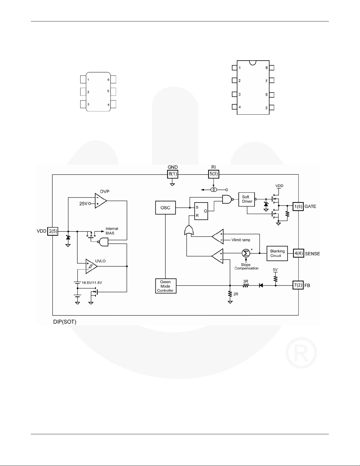
Pin Configuration
GND
FB
RI
Figure 1. SOT-26 Pin Configuration Figure 2. 8-Lead DIP Pin Configuration
Block Diagram
GATE
VDD
SENSE
GATE
VDD
NC
SENSE
GND
FB
NC
RI
Figure 3. DIP-8 Pin Assignment (Numbers in Parenthesis are SOT-26 Pin Assignment)
© 2006 Fairchild Semiconductor Corporation www.fairchildsemi.com
Rev. 1.0.1 • 10/9/08 2

AN-6858 APPLICATION NOTE
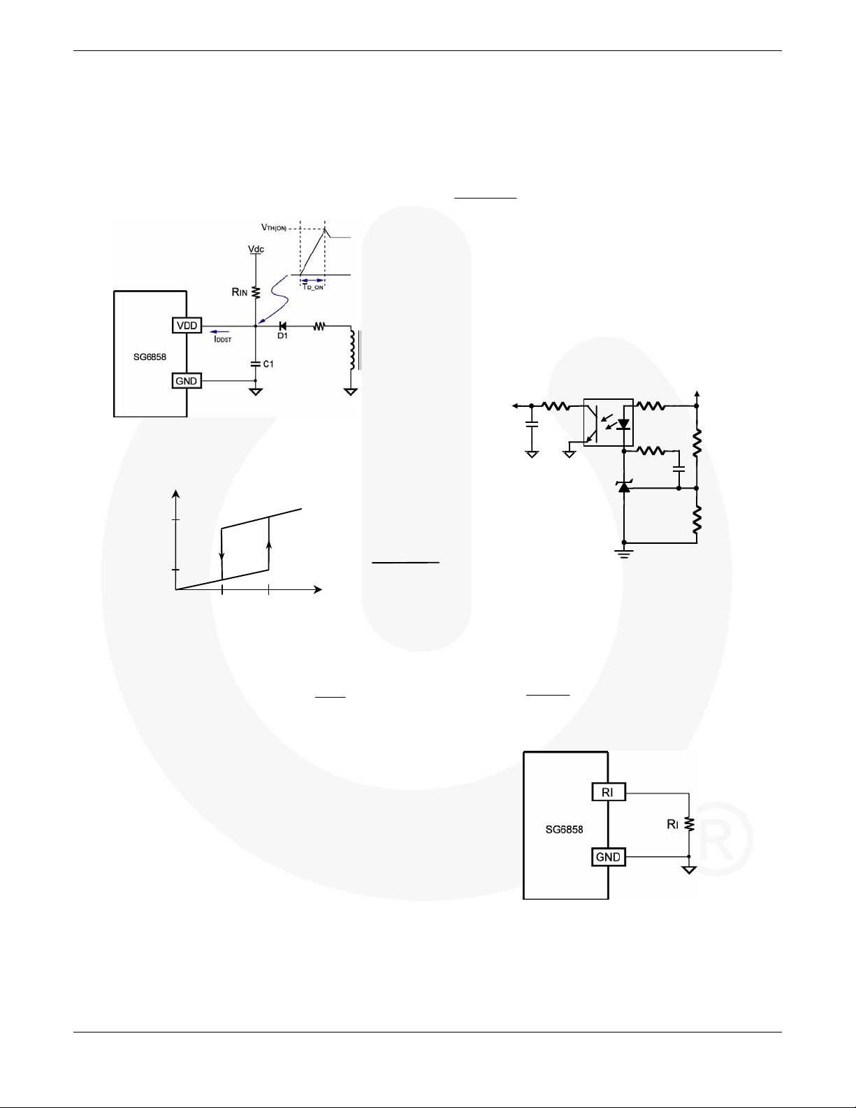
Startup Circuitry
When the power is turned on, the input rectified voltage,
V
, charges the hold-up capacitor C1 via startup resistor
DC
R
. As the voltage of the VDD pin reaches the start
IN
threshold voltage V
supply.
Figure 4. Circuit Providing Power
IDD
, SG6858 activates the entire power
DD-ON
.
from the FB pin to GND can increase stability. The
maximum source current on the FB pin is 2mA. The
phototransistor must be capable of sinking this current to
pull the FB level down at no load. The value of the biasing
resistor R
is determined as:
b
VVV
−−
ZDO
R
b
2≥×
mAK
(2)
where:
V
is the drop voltage of a photodiode, about 1.2V;
D
V
is the minimum operating vol tage of the shunt r egulator
Z
(typical 2.5V); and
K is the current transfer rate (CTR) of the opto-coupler.
For an output voltage V
maximum value of R
FB
RFB
CFB
= 5V with CTR = 100%, the
O
is 650Ω.
b
V
O
R
R3
b
C1
R1
2.5mA
R2
10µA
V
DD
11.5V 16.5V
Figure 5. UVLO Specification
The maximum power-on delay time is determined as:
t
_
OND
⎡
()
−−
⎢
1
eRIVV
−×−=
INSTDDDCONDD
⎢
⎣
⎤
−
×
1
CR
IN
⎥
⎥
⎦
(1)
Oscillator and Green Mode
One external resistor, RI, connected between the RI and
GND pins is used to program the PWM frequency of the
SG6858. The approximated formula is:
()
KHzf
OSC
The recommended f
Figure 6. Feedback Circuit
6650
()
Ω=KR
I
is from 50 to 100KHz.
OSC
(3)
where:
I
is the startup current and
DDST
t
is the power-on delay of the power supply.
D_ON
Due to the low start-up current, a large R
such as 1.5MΩ,
IN,
can be used. With a hold-up capacitor of 10µF/50V, the
power-on delay t
FB Input
is less than 2.8s for 90VAC input.
D_ON
Figure 7. Setting PWM Frequency
This pin is designed for feedback control and to activate
green mode. Figure 6 is a typical feedback circuit mainly
consisting of a shunt re gulator and an o pto-coupler . R1 and
R2 form a voltage divid er for the outp ut voltage regul ation.
R3 and C1 are adjusted for control-loop compensation. A
small-value RC filter (e.g. RFB= 47Ω, C
© 2006 Fairchild Semiconductor Corporation www.fairchildsemi.com
Rev. 1.0.1 • 10/9/08 3
= 1nF) placed
FB
The proprietary green mode provides off-time modulation to
reduce the PWM frequency in light-load and no-load
conditions. The feedback voltage of the FB pin is taken as a
reference. When the feedback voltage is lower than about
2.85V, the PWM frequency decreases. Because most losses
in a switching-mode power supply are proportional to the
 Loading...