Fairchild SG6846B service manual

SG6846B
Highly Integrated Green-Mode PWM Controller
SG6846B — Highly Integrated Green-Mode PWM Controller
October 2008
Features
Low Startup Current: 8µA
Low Operating Current: 3.7mA
Peak-Current Mode Operation with Cycle-by-cycle
Current Limiting
PWM Frequency Continuously Decreasing with
Burst Mode at Light Loads
V
Over Voltage Protection (OVP)
DD
AC Input Brownout Protection with Hysteresis
Constant Output Power Limit (Full AC Input Range)
Internal Latch Circuit for OVP, OTP, and OCP
(BLSY, BLSZ)
Two-level OCP Delay with 200ms
Programmable PWM Frequency with Frequency
Hopping
OCP Threshold is 2/3 Peak Current Limit
Soft Startup Time: 5ms
Applications
General-purpose switch-mode power supplies and
flyback power converters, including:
Power Adapters
Open-frame SMPS
SMPS with Surge-current Output, such as for
Printers, Scanners, Motor Drivers
Description
The highly integrated PWM controller, SG6846B,
provides several features to enhance the performance
of fly-back converters. To minimize standby power
consumption, a proprietary green-mode function
provides off-time modulation to continuously decrease
the switching frequency under light-load conditions.
Under zero-load conditions, the power supply enters
burst-mode. This completely shuts off PWM output. If
V
is larger than around 1.6V, PWM pulses out. This
FB
green-mode function enables power supplies to meet
international power conservation requirements.
The SG6846B is designed for SMPS with surge-current
output. It is incorporated with a two-level OCP function.
Besides, the cycle-by-cycle current limiting, if the
switching current is higher than OCP threshold and
lasts for 200ms, SG6846B stops gate immediately and
latches itself (BLSY version) or restarts after V
charges up to 16.5V (BCSY version). SG6846B also
integrates frequency-hopping function internally. The
frequency hopping function helps reduce EMI emission
of a power supply with minimum line filters. It has builtin synchronized slope compensation, proprietary
internal compensation for constant output power limit
over universal AC input range. The gate output is
clamped at 18V to protect the external MOSFET from
over-voltage damage.
Protection include: AC input brownout protection with
hysteresis and V
temperature protection, an external NTC thermistor can
be applied to sense the ambient temperature. When
OCP, V
circuit is used to latch-off the controller. The latch resets
when V
SG6846B is available in 8-pin SOP package.
OVP, or OTP are activated, an internal latch
DD
supply is removed.
DD
over-voltage protection. For over-
DD
DD
Ordering Information
Part
Number
SG6846BLSY -40 to +105°C Yes Green 8-Pin Small Outline Package (SOP) Tape & Reel
SG6846BLSZ -40 to +105°C Yes RoHS 8-Pin Small Outline Package (SOP) Tape & Reel
SG6846BCSY -40 to +105°C No Green 8-Pin Small Outline Package (SOP) Tape & Reel
SG6846BCSZ -40 to +105°C No RoHS 8-Pin Small Outline Package (SOP) Tape & Reel
For Fairchild’s definition of “green” Eco Status, please vis i t : http://www.fairchildsemi.com/company/green/rohs_green.html.
© 2008 Fairchild Semiconductor Corporation www.fairchildsemi.com
SG6846B • Rev. 1.3.4
Operating
Temperature Range
OCP
Latch
Eco
Status
Package
Packing
Method

Typical Application
L
AC input
N
EMI
Filter
3
7
VINRIVDD GATE
SG6846B — Highly Integrated Green-Mode PWM Controller
+
+
+
8
+
VO+
VO-
Block Diagram
0.9V/0.7V
VIN
3
7
VDD
4
2
FB
V
DD
-TH-G
UVLO
16.5V/10.5V
6
SENSE
GND
RT
5
1
SG6846B
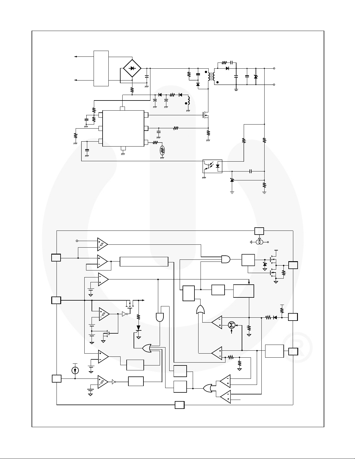
Figure 1. Typical Application
Over Power Compersation
0.895-0.065
Internal
BIAS
Latch
XVIN
4
VDD
Soft
Driver
Slope
1R
Green
Mode
+
3R
1R
Blanking
Circuit
S
Q
R
OSC
Compensation
6.2V
8
2
6
GATE
FB
SENSE
2R
1.15V
RT
23.6V
I
RT
5
1.05V
Debounce
OTP
Delay
SCP
Delay
OCP
Delay
1
GND
Figure 2. Block Diagram
© 2008 Fairchild Semiconductor Corporation www.fairchildsemi.com
SG6846B • Rev. 1.3.4 2

Marking Information
SG6846BFTP
XXXXXXXXYWWV
※ Marking for SG6846BLSZ (Pb-free)
SG6846BCSZ (Pb-free)
SG6846B — Highly Integrated Green-Mode PWM Controller
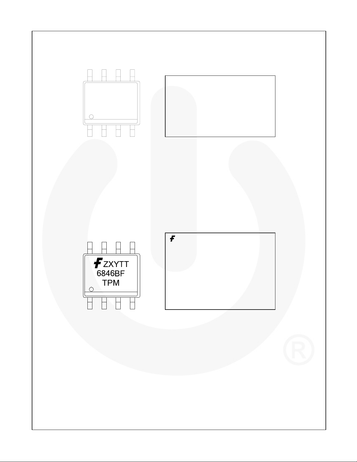
F: L = OCP Latch, C = OCP auto-recovery
T: S = SOP
P: Z = Lead Free + ROHS Compatible
Null = regular package
XXXXXXXX: Wafer Lot
Y: Year; WW: Week
V: Assembly Location
Figure 3. Top Mark 1
: Fairchild logo
Z: Plant Code
X: Year Code
Y: Week Code
TT: Die Run Code
F: L = OCP Latch, C = OCP auto-recovery
T: Package type, S = SOP
Green Package
P: Y =
M: Manufacturing flow code
※ Marking for SG6846BLSY (Green-compound)
SG6846BCSY (Green-compound)
Figure 4. Top Mark 2
© 2008 Fairchild Semiconductor Corporation www.fairchildsemi.com
SG6846B • Rev. 1.3.4 3

Pin Configuration
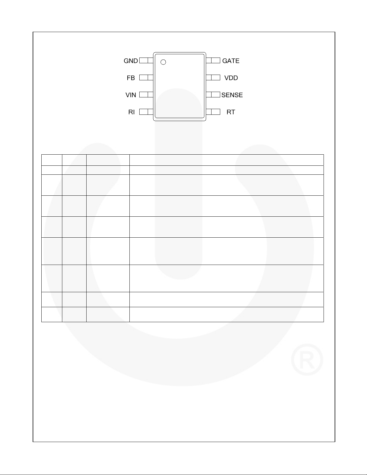
Figure 5. Pin Configuration
Pin Definitions
Pin # Name Function Description
1 GND Ground Ground.
The signal from the external compensation circuit is fed into this pin. The PWM
2 FB Feedback
3 VIN
4 RI
5 RT
6 SENSE Current Sense
7 VDD Power Supply
8 GATE Driver Output
Line-voltage
Detection
Reference
Setting
Temperature
Detection
duty cycle is determined in response to the signal from this pin and the currentsense signal from pin 6.
Line-voltage detection is used for brownout protection with hysteresis. Constant
output power limit over universal AC input range is achieved using this pin. Add
a low-pass filter to filter out line ripple on the bulk capacitor.
A resistor from the RI pin to ground generates a reference current source that
determines the switching frequency. Increasing the resistance reduces the
switching frequency. A 26k resistor results in a 65kHz switching frequency.
For over-temperature protection, an external NTC thermistor is connected from
this pin to the GND pin. The impedance of the NTC decreases at high
temperatures. Once the voltage of the RT pin drops below a threshold, PWM
output is disabled.
The sensed voltage is used for peak-current-mode control and cycle-by-cycle
current limiting. If the switching current is higher than OCP threshold and lasts
for 200ms, SG6846B turns off immediately. This two-level OCP feature is
especially suitable for SMPS with surge current output.
If an open-circuit failure occurs in the feedback loop, the internal protection
circuit disables PWM output as long as V
The totem-pole output driver for the power MOSFET; internally clamped
below 18V.
exceeds a threshold.
DD
SG6846B — Highly Integrated Green-Mode PWM Controller
© 2008 Fairchild Semiconductor Corporation www.fairchildsemi.com
SG6846B • Rev. 1.3.4 4

SG6846B — Highly Integrated Green-Mode PWM Controller
Absolute Maximum Ratings
Stresses exceeding the absolute maximum ratings may damage the device. The device may not function or be
operable above the recommended operating conditions and stressing the parts to these levels is not recommended.
In addition, extended exposure to stresses above the recommended operating conditions may affect device
reliability. The absolute maximum ratings are stress ratings only. All voltage values, except differential voltages, are
given with respect to GND pin.
Symbol Parameter Min. Max. Unit
VDD Supply Voltage 30 V
VL Input Voltage to FB, SENSE, VIN, RT, RI Pins -0.3 7.0 V
PD Power Dissipation at TA<50°C SOP 400 mW
JC Thermal Resistance (Junction-to-Case) SOP 54.4 °C/W
TJ Operating Junction Temperature -40 +150 °C
T
Storage Temperature Range -65 +150 °C
STG
TL Lead Temperature, Wave Soldering, 10 Seconds +260 °C
ESD
Human Body Model, JESD22-A114 5.0
Charge Device Model, JESD22-C101 1.5
kV
Recommended Operating Conditions
The Recommended Operating Conditions table defines the conditions for actual device operation. Recommended
operating conditions are specified to ensure optimal performance to the datasheet specifications. Fairchild does not
recommend exceeding them or designing to Absolute Maximum Ratings.
Symbol Parameter Min. Max. Unit
TA Operating Ambient Temperature -40 +105 °C
© 2008 Fairchild Semiconductor Corporation www.fairchildsemi.com
SG6846B • Rev. 1.3.4 5
 Loading...