Fairchild SG6741A, SG6741A Schematic [ru]

SG6741A
Highly Integrated Green-Mode PWM Controller
SG6741A — Highly Integrated Green-Mode PWM Controller
August 2010
Features
High-Voltage Startup
Low Operating Current: 4mA
Linearly Decreasing PWM Frequency to 18kHz
Frequency Hopping to Reduce EMI Emissions
Peak-Current-Mode Control
Cycle-by-Cycle Current Limiting
Leading-Edge Blanking (LEB)
Synchronized Slope Compensation
GATE Output Maximum Voltage Clamp: 18V
V
V
Over-Voltage Protection (Auto Restart)
DD
Under-Voltage Lockout (UVLO)
DD
Internal Open-Loop Protection
Constant Power Limit (Full AC Input Range)
Applications
General-purpose switch-mode power supplies and
flyback power converters, including:
Power Adapters
Open-Frame SMPS
Description
The highly integrated SG6741A series of PWM
controllers provides several features to enhance the
performance of flyback converters.
To minimize standby power consumption, a proprietary
green-mode function provides off-time modulation to
linearly decrease the switching frequency at light-load
conditions. To avoid acoustic-noise problems, the
minimum PWM frequency is set above 18KHz. This
green-mode function enables the power supply to meet
international power conservation requirements. With the
internal high-voltage startup circuitry, the power loss
due to bleeding resistors is eliminated. To further
reduce power consumption, SG6741A is manufactured
using the BiCMOS process, which allows an operating
current of only 4mA.
SG6741A integrates a frequency-hopping function
internally to reduce EMI emission of a power supply
with minimum line filters. A built-in synchronized slope
compensation achieves stable peak-current-mode
control. The proprietary internal line compensation
ensures constant output power limit over a wide AC
input voltages, from 90V
SG6741A provides many protection functions. In
addition to cycle-by-cycle current limiting, the internal
open-loop protection circuit ensures safety when an
open-loop or output short-circuit failure occurs. PWM
output is disabled until V
limit, when the controller starts up again. As long as V
exceeds ~26V, the internal OVP circuit is triggered.
SG6741A is available in an 8-pin SOP package.
to 264 VAC.
AC
drops below the UVLO lower
DD
DD
Ordering Information
Part Number
SG6741ASY -40 to +105°C 8-Lead Small Outline Package (SOP) Tape & Reel
© 2008 Fairchild Semiconductor Corporation www.fairchildsemi.com
SG6741A • Rev. 1.0.2
Operating
Temperature Range
Package Packing Method

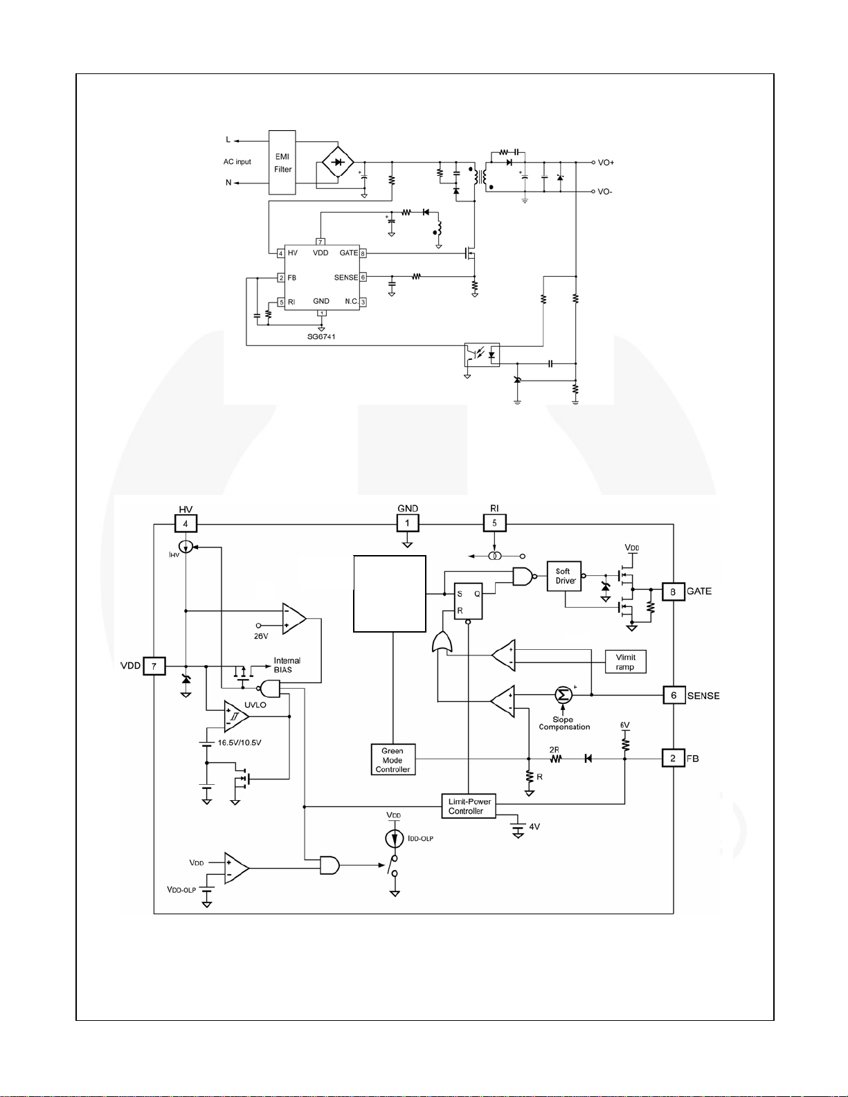
Application Diagram
SG6741A — Highly Integrated Green-Mode PWM Controller
Figure 1. Typical Application
Block Diagram
OSC
Generator
Figure 2. Block Diagram
© 2008 Fairchild Semiconductor Corporation www.fairchildsemi.com
SG6741A • Rev. 1.0.2 2

Marking Information
Pin Configuration
ZXYTT
6741A
TPM
GND
SG6741A — Highly Integrated Green-Mode PWM Controller
F: Fairchild Logo
Z: Plant Code
X: 1-Digit Year Code
Y: 1-Digit Week Code
TT: 2-Digit Die Run Code
T: Package Type (S = SOP)
P: Y=Green Package
M: Manufacture Flow Code
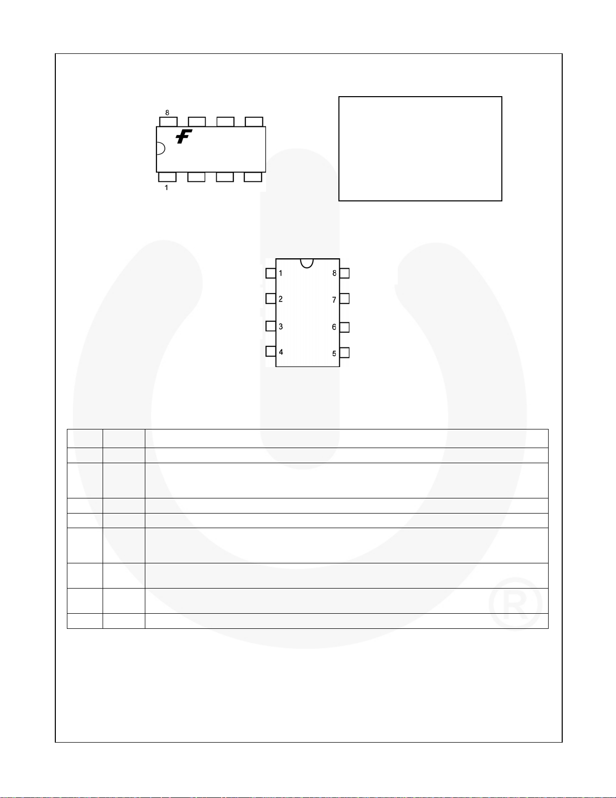
Figure 3. Top Mark
GATE
FB
NC
HV
Figure 4. Pin Configuration
VDD
SENSE
RI
Pin Definitions
Pin # Name Description
1 GND Ground.
Feedback. The signal from the external compensation circuit is fed into this pin. The PWM duty
2 FB
3 NC No Connection.
4 HV Startup Input. For startup, this pin is pulled HIGH to the line input or bulk capacitor via resistors.
5 RI
6 SENSE
7 VDD
8 GATE Driver Output. Totem-pole output driver. Soft driving waveform is implemented for improved EMI.
cycle is determined in response to the signal on this pin and the current-sense signal on SENSE
pin.
Reference Setting. A resistor connected from the RI pin to GND pin provides a constant current
source, which determines the center PWM frequency. Increasing the resistance reduces PWM
frequency. Using a 26KΩ resistor for R
Current Sense. The sensed voltage is used for peak-current-mode control and cycle-by-cycle
current limiting.
Power Supply. The internal protection circuit disables PWM output as long as V
OVP trigger point.
results in a 65kHz center PWM frequency.
I
DD
exceeds the
© 2008 Fairchild Semiconductor Corporation www.fairchildsemi.com
SG6741A • Rev. 1.0.2 3

SG6741A — Highly Integrated Green-Mode PWM Controller
Absolute Maximum Ratings
Stresses exceeding the absolute maximum ratings may damage the device. The device may not function or be
operable above the recommended operating conditions and stressing the parts to these levels is not recommended.
In addition, extended exposure to stresses above the recommended operating conditions may affect device
reliability. The absolute maximum ratings are stress ratings only. All voltage values, except differential voltages, are
given with respect to the ground pin.
Symbol Parameter Min. Max. Unit
V
DC Supply Voltage
VDD
VFB FB Pin Input Voltage -0.3 7.0 V
V
SENSE Pin Input Voltage -0.3 7.0 V
SENSE
VRI RI Pin Input Voltage -0.3 7.0 V
VHV HV Pin Input Voltage 500 V
PD
ΘJA
Power Dissipation
Thermal Resistance (Junction-to-Air) 141
TJ Operating Junction Temperature -40 +125
T
Storage Temperature Range -55 +150
STG
TL Lead Temperature (Wave Soldering or IR, 10 Seconds) +260
ESD
Electrostatic
Discharge Capability
Notes:
1. All voltage values, except differential voltages, are given with respect to the network ground terminal.
2. Stresses beyond those listed under Absolute Maximum Ratings may cause permanent damage to the device.
(1, 2)
30 V
(T
<50°C)
A
400 mW
°C/W
°C
°C
°C
Human Body Model, JESD22-A114,
All Pins Except HV Pin
Machine Model, JESD22-A115,
All Pins Except HV Pin
4 kV
200 V
© 2008 Fairchild Semiconductor Corporation www.fairchildsemi.com
SG6741A • Rev. 1.0.2 4
 Loading...