


December 2009
SG5842A/SG5842JA — Highly Integrated Green-Mode
PWM Controller
SG5842A/SG5842JA — Highly Integrated Green-Mode PWM Controller
Features
Green-Mode PWM Controller
Low Startup Current: 14µA
Low Operating Current: 4mA
Programmable PWM Frequency with Hopping
(SG5842JA)
Peak-Current-Mode Control
Cycle-by-Cycle Current Limiting
Synchronized Slope Compensation
Leading-Edge Blanking (LEB)
Constant Output Power Limit
Totem-Pole Output with Soft Driving
V
Over-Voltage Protection (OVP)
DD
Programmable Over-Temperature Protection (OTP)
Internal Latch Circuit (OTP, OVP)
Internal Open-Loop Protection
V
Under-Voltage Lockout (UVLO)
DD
GATE Output Maximum Voltage Clamp: 18V
Applications
General-purpose switch-mode power supplies and
flyback power converters, including:
Notebook Power Adapters
Open-Frame SMPS
Description
The highly integrated SG5842A/JA series of PWM
controllers provides several features to enhance the
performance of flyback converters. To minimize standby
power consumption, a proprietary green-mode function
provides off-time modulation to continuously decrease
the switching frequency at light-load conditions. To
avoid acoustic-noise problems, the minimum PWM
frequency set above 22KHz. This green-mode function
enables the power supply to meet international power
conservation requirements. To further reduce power
consumption, SG5842A/JA is manufactured using the
BiCMOS process. This allows a low startup current,
around 14µA, and an operating current of only 4mA. As
a result, a large startup resistance can be used.
The SG5842A/JA built-in synchronized slope
compensation achieves stable peak-current-mode
control. SG5842JA integrates a frequency-hopping
function that helps reduce EMI emission of a power
supply with minimum line filters.
SG5842A/JA provides many protection functions. In
addition to cycle-by-cycle current limiting, the internal
open-loop protection circuit ensures safety should an
open-loop or output short-circuit failure occur. PWM
output is disabled until V
limit, then the controller starts again. As long as V
exceeds about 24V, the internal OVP circuit is triggered.
An external NTC thermistor can be applied for overtemperature protection.
SG5842A/JA is available in an 8-pin DIP or SOP
package.
drops below the UVLO lower
DD
DD
© 2007 Fairchild Semiconductor Corporation www.fairchildsemi.com
SG5842A/SG5842JA • Rev. 1.4.3
Ordering Information
SG5842A/SG5842JA — Highly Integrated Green-Mode PWM Controller
Operating
Part Number
Temperature
Range
SG5842JASZ -40°C to +105°C RoHS
SG5842JADZ -40°C to +105°C RoHS
SG5842JASY -40°C to +105°C Green
SG5842ASZ
(Preliminary)
SG5842ASY
(Preliminary)
For Fairchild’s definition of Eco Status, please vis i t: http://www.fairchildsemi.com/company/green/rohs_green.html.
-40°C to +105°C RoHS
-40°C to +105°C Green
Eco
Status
Package
8-Pin Small Outline Package (SOP)
8-Pin Dual Inline Package (DIP)
8-Pin Small Outline Package (SOP)
8-Pin Small Outline Package (SOP)
8-Pin Small Outline Package (SOP)
OTP
Latch
Yes Yes Yes
Yes Yes Yes
Yes Yes Yes
Yes Yes No
Yes Yes No
OVP
Latch
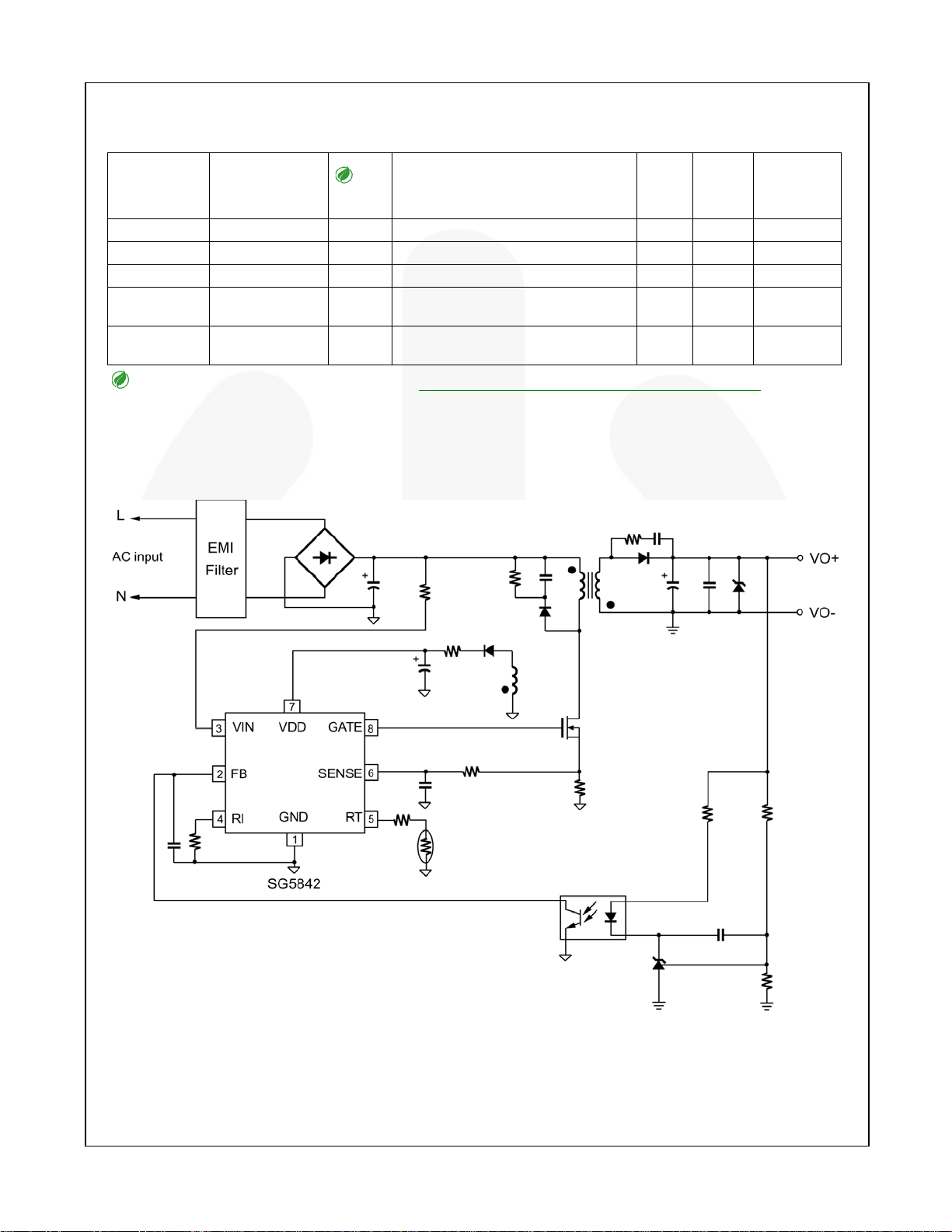
Application Diagram
Frequency
Hopping
Figure 1. Application Diagram
© 2007 Fairchild Semiconductor Corporation www.fairchildsemi.com
SG5842A/SG582JA • Rev. 1.4.3 2
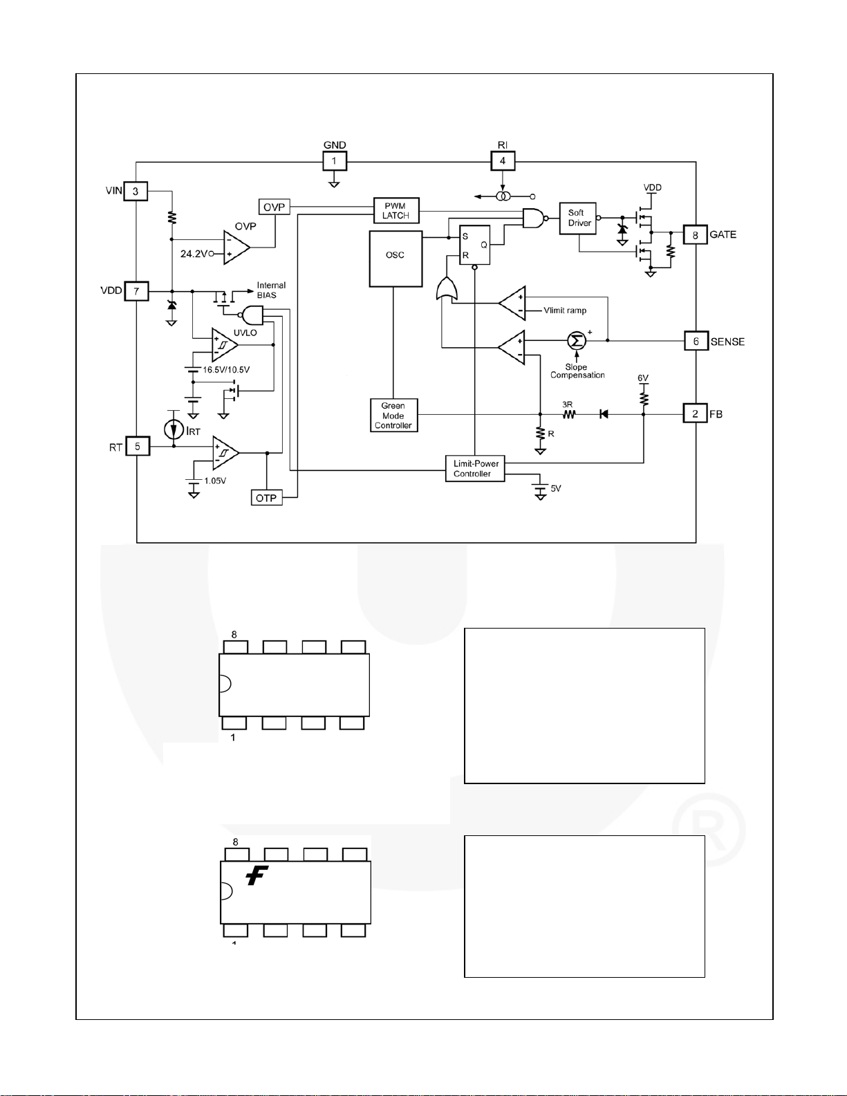
Block Diagram
SG5842A/SG5842JA — Highly Integrated Green-Mode PWM Controller
Marking Information
Marking for SG5842JASZ (pb-free)
Marking for SG5842JADZ (pb-free)
Marking for SG5842ASZ (pb-free)
Marking for SG5842ADZ (pb-free)
Marking for SG5842JASY (green-compound)
Marking for SG5842ASY (green-compound)
SG5842HATP
XXXXXXXXYWW V
Figure 2. Function Block Diagram
ZXYTT
SG5842HA
TPM
H: J = with Frequency Hopping
Null = without Frequency
Hopping
T: D = DIP, S = SOP
P: Z = Lead Free
Null = Regular Package
XXXXXXXX: Wafer Lot
Y: Year; WW: Week
V: Assembly Location
F- Fairchild Logo
Z- Plant Code
X- 1 Digit Year Code
Y- 1 Digit week Code
TT: 2 Digits Die Run Code
T: Package Type (S=SOP, D=DIP)
P: Y: Green Package
M: Manufacture Flow Code
Figure 3. Top Mark
© 2007 Fairchild Semiconductor Corporation www.fairchildsemi.com
SG5842A/SG582JA • Rev. 1.4.3 3
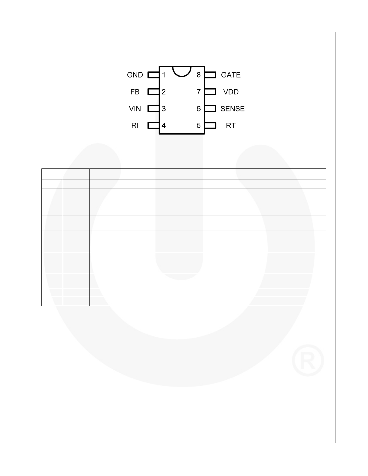
Pin Configuration
Figure 4. Pin Configuration
Pin Definitions
Pin # Name Description
1 GND Ground
The signal from the external compensation circuit is fed into this pin. The PWM duty cycle is
2 FB
3 VIN
4 RI
5 RT
6 SENSE
7 VDD Power supply. The internal protection circuit disables PWM output if VDD is over-voltage.
8 GATE The totem-pole output driver for the power MOSFET, which is internally clamped below 18V.
determined in response to the signal from this pin and the current-sense signal from Pin 6. If FB
voltage exceeds the threshold, the internal protection circuit disables PWM output after a
predetermined delay time.
For startup, this pin is pulled HIGH to the rectified line input via a resistor. Since the startup
current requirement is very small, a large startup resistance can be used to minimize power loss.
A resistor connected from the RI pin to GND provides a constant current source. This determines
the center PWM frequency. Increasing the resistance reduces PWM frequency. Using a 26KΩ
resistor results in a 65KHz center PWM frequency.
For over-temperature protection. An external NTC thermistor is connected from this pin to the
GND pin. The impedance of the NTC decreases at high temperatures. Once the voltage of the
RT pin drops below a fixed limit, PWM output is latched off.
Current sense. The sensed voltage is used for peak-current-mode control and cycle-by-cycle
current limiting.
SG5842A/SG5842JA — Highly Integrated Green-Mode PWM Controller
© 2007 Fairchild Semiconductor Corporation www.fairchildsemi.com
SG5842A/SG582JA • Rev. 1.4.3 4
SG5842A/SG5842JA — Highly Integrated Green-Mode PWM Controller
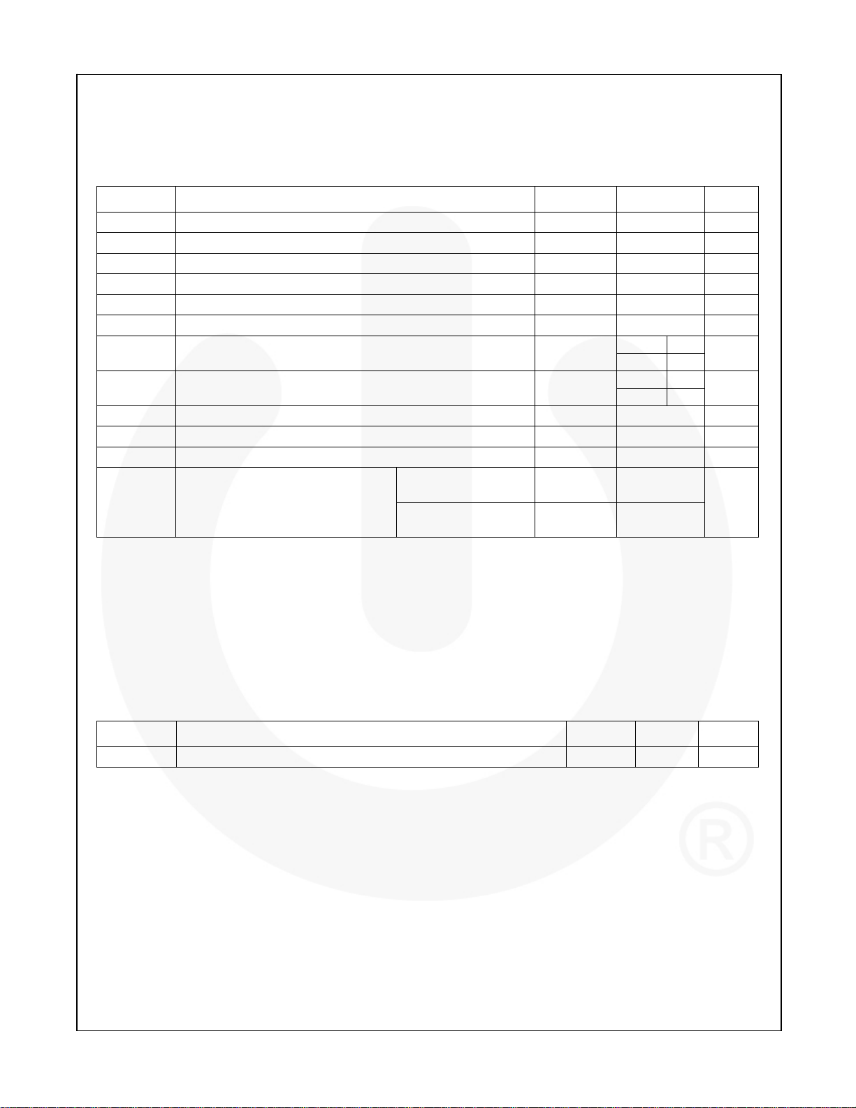
Absolute Maximum Ratings
Stresses exceeding the absolute maximum ratings may damage the device. The device may not function or be
operable above the recommended operating conditions and stressing the parts to these levels is not recommended.
In addition, extended exposure to stresses above the recommended operating conditions may affect device
reliability. The absolute maximum ratings are stress ratings only.
Symbol Parameter Min. Max. Unit
V
Supply Voltage
VDD
V
Input Terminal 30
VIN
VFB Input Voltage to FB Pin -0.3 7.0
V
Input Voltage to SENSE Pin -0.3 7.0
SENSE
VRT Input Voltage to RT Pin -0.3 7.0
VRI Input Voltage to RI Pin -0.3 7.0
PD Power Dissipation (TA < 50°C )
ΘJA
Thermal Resistance (Junction-to-Air)
TJ Operating Junction Temperature -40 +125
T
Storage Temperature Range -55 +150
STG
T
L
Lead Temperature (Wave Soldering or Infrared, 10 Seconds) +260
ESD Electrostatic Discharge Capability
Notes:
1. All voltage values, except differential voltage, are given with respect to GND pin.
2. Stresses beyond those listed under Absolute Maximum Ratings may cause permanent damage to the device.
(1)
30
V
V
V
V
V
V
DIP 800
SOP 400
DIP 82.5
SOP 141
mW
°C/W
°C
°C
°C
Human Body Model,
JESD22-A114
Charged Device
Model, JESD22-C101
3
KV
1
Recommended Operating Conditions
The Recommended Operating Conditions table defines the conditions for actual device operation. Recommended
operating conditions are specified to ensure optimal performance to the datasheet specifications. Fairchild does not
recommend exceeding them or designing to Absolute Maximum Ratings.
Symbol Parameter Min. Max. Unit
TA Operating Ambient Temperature -20 +85 °C
© 2007 Fairchild Semiconductor Corporation www.fairchildsemi.com
SG5842A/SG582JA • Rev. 1.4.3 5
 Loading...