

www.fairchildsemi.com
Reference Design RD-310
Primary-Side-Regulation PWM with POWER MOSFET – 3.5W
Design
Featured Device Application
FSEZ1317
Cell Phone
Charger
Input Voltage
Range
90~265V
AC
Output Voltage
(Rated Current)
5V (0.7A) 3.5W
Rated Output
Power
Key Features
Low Standby Power Under 30mW
High Voltage Startup
Constant-Voltage (CV) and Constant-Current (CC) Control without Secondary-Feedback
Circuitry
Green Mode Function: Frequency Reduction at Light-Load
Fixed PWM Frequency at 50kHz with Frequency Hopping to Reduce EMI
Cable Voltage Drop Compensation in CV Mode
Various Protection Functions: V
(UVLO), and Over-Temperature Protection (OTP)
Over-Voltage Protection (OVP), VDD Under-Voltage Lockout
DD
7-Lead Small Outline Package (SOP)
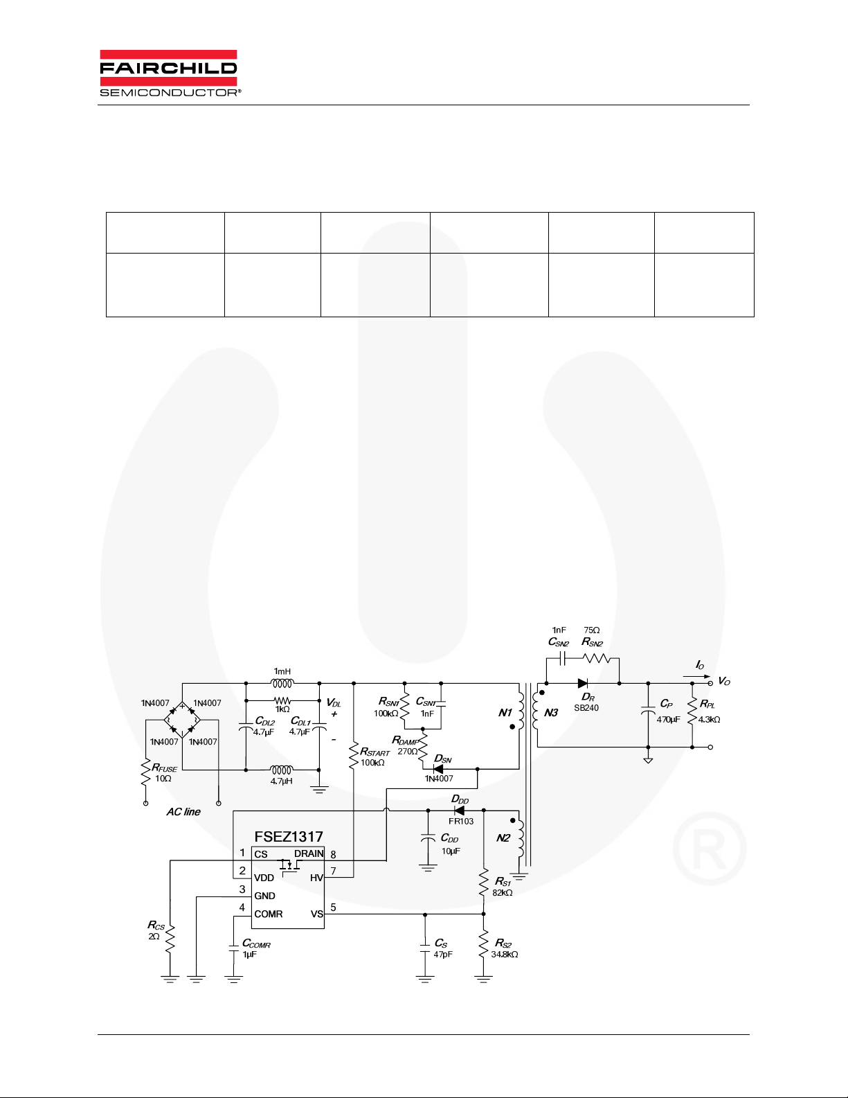
1. Schematic
Topology
Primary-Side
Regulated
Flyback
Converter
Figure 1. Schematic
© 2009 Fairchild Semiconductor Corporation 1 RD-310_FSEZ1317 • Rev. 0.0.2
www.fairchildsemi.com
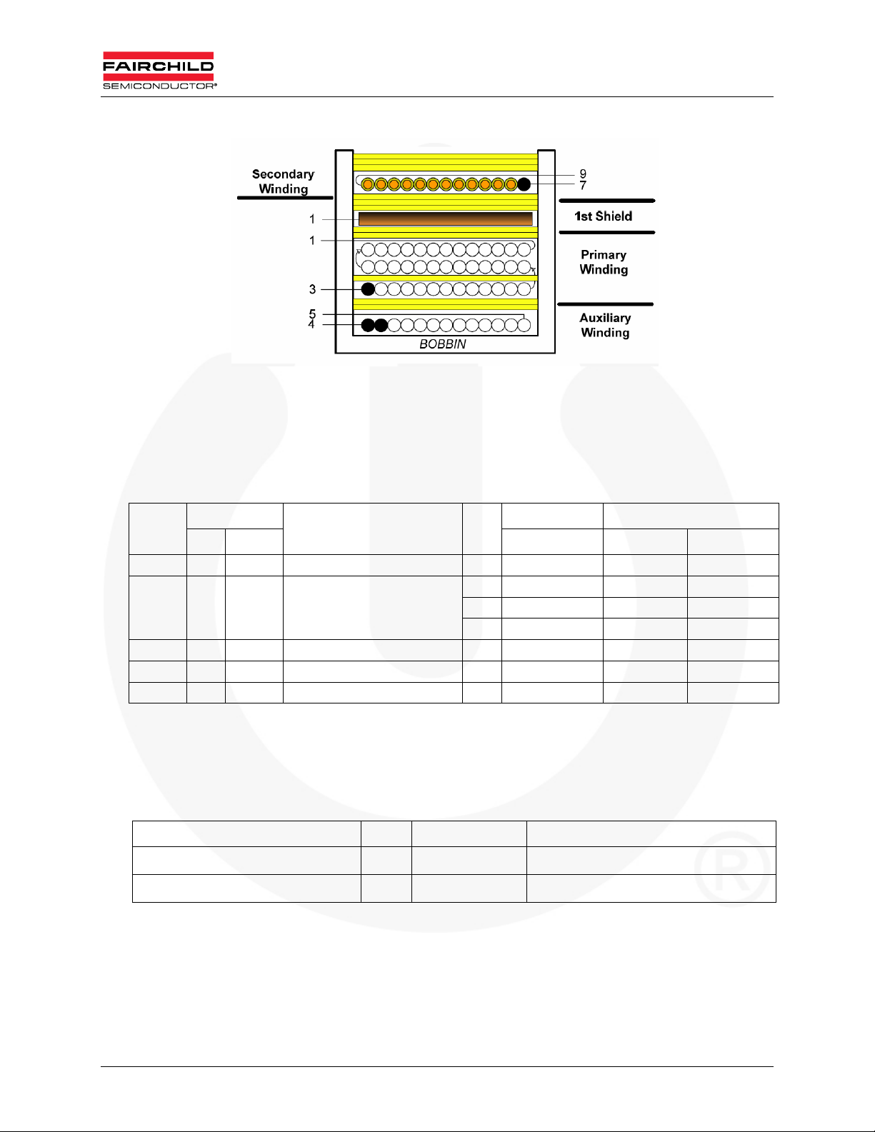
2. Transformer
Figure 2. Transformer Schematic Diagram
Notes:
1. When W4R’s winding is reversed winding, it must wind one layer.
2. When W2 is winding, it must wind three layers and put one layer of tape after winding the first
layer.
2.1. Winding Specification
No.
W1 4 5 2UEW 0.23*1 15 2
W2 3 1 2UEW 0.18*1
W3 1 COPPER SHIELD 1.2 3
W4 7 9 TEX-E 0.55*1 9 3
CORE ROUNDING TAPE 3
Terminal
Wire ts
S F ts Primary Seconds
41 1
39 0
37 2
Insulation Barrier Tape
Core: EE16
Bobbin: EE16
2.2. Electrical Characteristics
Pin Specification Remark
Primary-Side Inductance 1-3 2.25mH ± 5% 100kHz, 1V
Primary-Side Leakage Inductance
1-3
80μH Maximum
Short One of the Secondary Windings
© 2009 Fairchild Semiconductor Corporation 2 RD-310_FSEZ1317 • Rev. 0.0.2

www.fairchildsemi.com
y
V
3. Typical Performance
74.00%
0.05
72.00%
0.04
70.00%
68.00%
0.03
66.00%
0.02
64.00%
62.00%
0.01
60.00%
58.00%
0.175 0.35 0.525 0.7
Figure 3. Efficienc
Figure 4. Input Power vs. Input Voltage
0
90 120 150 180 210 240 270
Figure 5. Output
oltage vs. Output Current
© 2009 Fairchild Semiconductor Corporation 3 RD-310_FSEZ1317 • Rev. 0.0.2

www.fairchildsemi.com
4. Related Resources
FSEZ1317 — Primary-Side-Regulation PWM with POWER MOSFET Integrated Datasheet
AN-6067 — Design and Application of Primary-Side Regulation (PSR) PWM Controller
Reference Design Disclaimer
Fairchild Semico nductor Corp oration (“ Fairchild”) provides thes e refere nce design servi ces as a be nefit to our c ustomers. Fai rchild ha s made a go od
faith attempt to build for the specifi cations provided or needed by the cust omer. Fairchild provi des this product “a s is” and without “reco urse” and
MAKES NO WARRANTY, EXPRESSED, IMPLIED OR OTHERWISE, INCLUDING ANY WARRANTY OF MERCHANTABILITY AND FITNESS FOR A
PARTICULAR PURPOSE.
Customer agrees to do its own testing of any Fairchild referen ce designs in order t o ensure design m eets the customer n eeds. Neither Fairchild nor
Customer shall be liabl e fo r i nci de ntal o r con seq ue ntial dam a ges , incl u din g b ut not l im ite d to, the cost of labor, re-qualifications, rework cha rges, d ela y,
lost profits, or loss of goodwill arising out of the sale, installation or use of any Fairchild product.
Subject to the limitations herein, Fairchild will defend any suit or proceeding brought against Customer if it is based o n a claim that any p roduct
furnished hereun der constitutes an i nfringement of an y intellectual propert y rights. Fairchild must be notified prom ptly in writing an d given full and
complete authority, informati on and assistance (at Fairchild’s expense) for defens e of the suit. Fairchild will pay damages an d costs ther ein award ed
against Customer b ut shall not be responsibl e for a ny com promise ma de wit hout i ts consen t. In no event sh all Fai rchild’s l iabilit y for all dama ges and
costs (including the c osts of the defen se by Fairchild) e xceed the contra ctual value of t he products or servi ces that are the subject of the la wsuit. In
providing such defen se, or in the event that such product is hel d to constitute infringement and the use of the product is enjoined, Fairc hild, in its
discretion, shall procure the right to continue using such product, or modify it so that it becomes noninfringing, or remove it and grant Custo m er a credit
for the depreciate d value ther eof. Fairchil d’s indemnit y does not extend to clai ms of infrin gement arisi ng from Fai rchild’s compl iance with Cust omer’s
design, specifications an d/or instructi ons, or the use of any p roduct in c ombi nation with othe r prod ucts or i n connec tion with a man ufactu ring or other
process. The fore going rem edy is e xclusive and constitutes F airchild’s sol e obligati on for any claim of i ntellectual propert y infringem ent and Fairchild
makes no warranty that products sold hereunder will not infringe any intellectual property rights.
All solutions, designs, schematics, drawings, boards or other information provided by Fairchild to Customer are confidential and provided for
Customer’s own use. Customer may not share any Fairchild materials with other semiconductor suppliers.
© 2009 Fairchild Semiconductor Corporation 4 RD-310_FSEZ1317 • Rev. 0.0.2
 Loading...