

查询RC4558供应商
RC4558
Dual High-Gain Operational Amplifier
Features
• 2.5 MHz unity gain bandwidth
• Supply voltage ±22V for RM4558 and ±18V for
RC/RV4558
• Short-circuit protection
• No frequency compensation required
Description
The RC4558 integrated circuit is a dual high-gain operational amplifier internally compensated and constructed on a
single silicon IC using an advanced epitaxial process.
• No latch-up
• Large common-mode and differential voltage ranges
• Low power consumption
• Parameter tracking over temperature range
• Gain and phase match between amplifiers
www.fairchildsemi.com
Combining the features of the 741 with the close parameter
matching and tracking of a dual device on a monolithic chip
results in unique performance characteristics. Excellent
channel separation allows the use of this dual device in dense
single 741 operational amplifier applications. It is especially
well suited for applications in differential-in, differential-out
as well as in potentiometric amplifiers and where gain and
phase matched channels are mandatory.
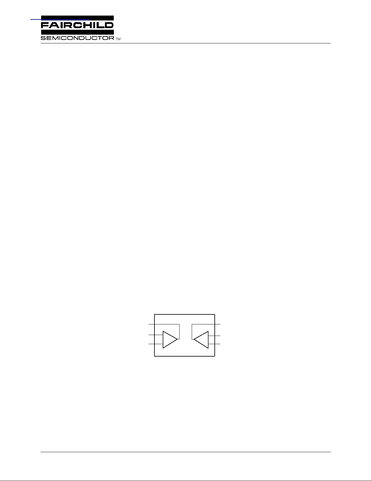
Block Diagram
Output (A)
–Input (A)
–Input (A)
_
A
+
_
B
+
65-4558-01
Output (B)
–Input (B)
+Input (B)
Rev. 1.0.0
PRODUCT SPECIFICATION RC4558
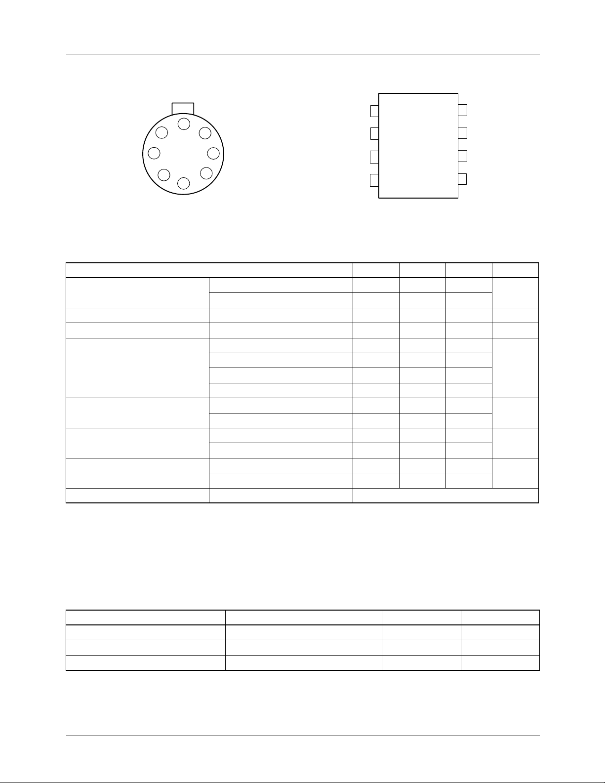
Pin Assignments
+V
S
Output (A)
Output (A)
8
1
7
Output (B)
–Input (A)
1
2
8
7
+V
S
Output (B)
–Input (A)
+Input (A)
2
3
4
–V
6
–Input (B)
5
+Input (B)
S
65-3473-02
+Input (A)
–V
3
4
S
6
5
65-3473-03
Absolute Maximum Ratings
(beyond which the device may be damaged)
Parameter Min Typ Max Units
Supply Voltage RM4558 ±22 V
RC4558 ±18
Input Voltage
2
Differential Input Voltage 30 V
PDTA < 50°C SOIC 300 mW
PDIP 468
CerDIP 833
TO-99 658
Junction Temperature SOIC, PDIP 125 °C
CerDIP, TO-99 175
Operating Temperature RM4558 -55 125 °C
RC4558 0 70
Lead Soldering Temperature PDIP, CerDIP, TO-99 (60 sec) 300 °C
SOIC (10 sec) 260
Output Short Circuit Duration
Notes:
1. Functional operation under any of these conditions is NOT implied.
2. For supply voltages less than ±15V, the absolute maximum input voltage is equal to the supply voltage.
3. Short circuit may be to ground on one op amp only. Rating applies to +75°C ambient temperature.
3
1
±15 V
Indefinite
–Input (B)
+Input (B)
Matching Characteristics
(VS = ±15V, TA = +25°C unless otherwise specified)
Parameter Test Conditions Typ Units
Voltage Gain RL ³ 2 kW±1.0 dB
Input Bias Current RL ³ 2 kW±15 nA
Input Offset Current RL ³ 2 kW±7.5 nA
2
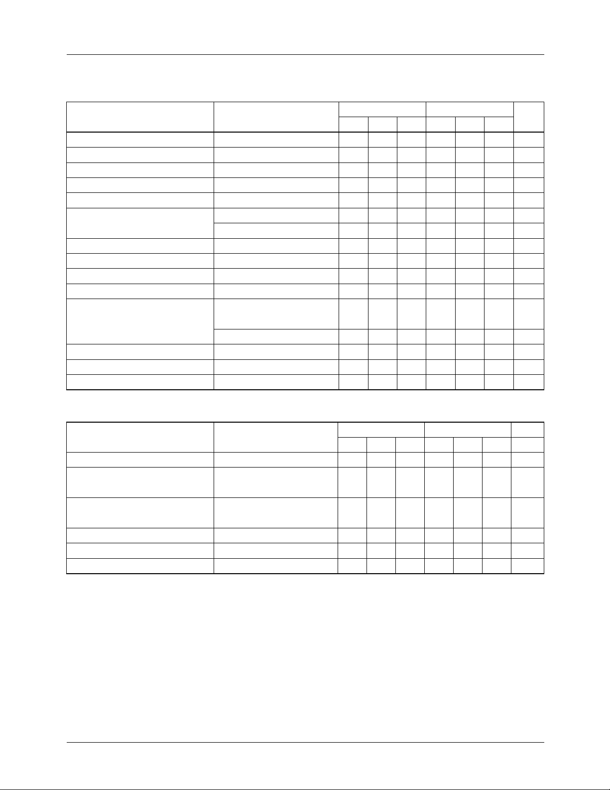
RC4558 PRODUCT SPECIFICATION
Electrical Characteristics
(VS = ±15V and TA = +25°C unless otherwise specified)
RM4558 RC4558
Parameters Test Conditions Min Typ Max Min Typ Max Units
Input Offset Voltage R
Input Offset Current 5.0 200 5.0 200 nA
Input Bias Current 40 500 40 500 nA
Input Resistance 0.3 1.0 0.3 1.0 MW
Large Signal Voltage Gain RL ³ 2kW, V
Output Voltage Swing R
Input Voltage Range ±12 ±13 ±12 ±13 V
Common Mode Rejection Ratio RS £ 10kW 70 100 70 100 dB
Power Supply Rejection Ratio RS £ 10kW 76 100 76 100 dB
Power Consumption RL = ¥ 100 170 100 170 mW
Transient Response VIN = 20 mV
Rise Time RL = 2kW 0.3 0.3 mS
Overshoot CL £ 100pF 35 35 %
Slew Rate R
Channel Separation F = 10kHz, RS = 1kW 90 90 dB
Unity Gain Bandwidth (Gain = 1) 2.5 3.0 2.0 3.0 MHz
£ 10kW 1.0 5.0 2.0 6.0 mV
S
= ±10V 50 300 20 300 V/mV
OUT
³ 10kW±12 ±14 ±12 ±14 V
L
RL ³ 2kW±10 ±13 ±10 ±13 V
³ 2kW 0.8 0.8 V/mS
L
The following specifications apply for RM = -55°C £ T
£ +125°C, RC = 0° £ TA £ +70°C
A
RM4558 RC4558
Parameters Test Conditions
Input Offset Voltage R
£ 10kW 6.0 7.5 mV
S
Min Typ Max Min Typ Max Units
Input Offset Current
RC4558 500 300 nA
Input bias Current
RC4558 1500 800 nA
Large Signal Voltage Gain RL ³ 2kW, V
= ±10 25 15 V/mV
OUT
Output Voltage Swing RL ³ 2kW±10 ±10 V
Power Consumption RL = ¥ 120 200 120 200 mW
3
PRODUCT SPECIFICATION RC4558
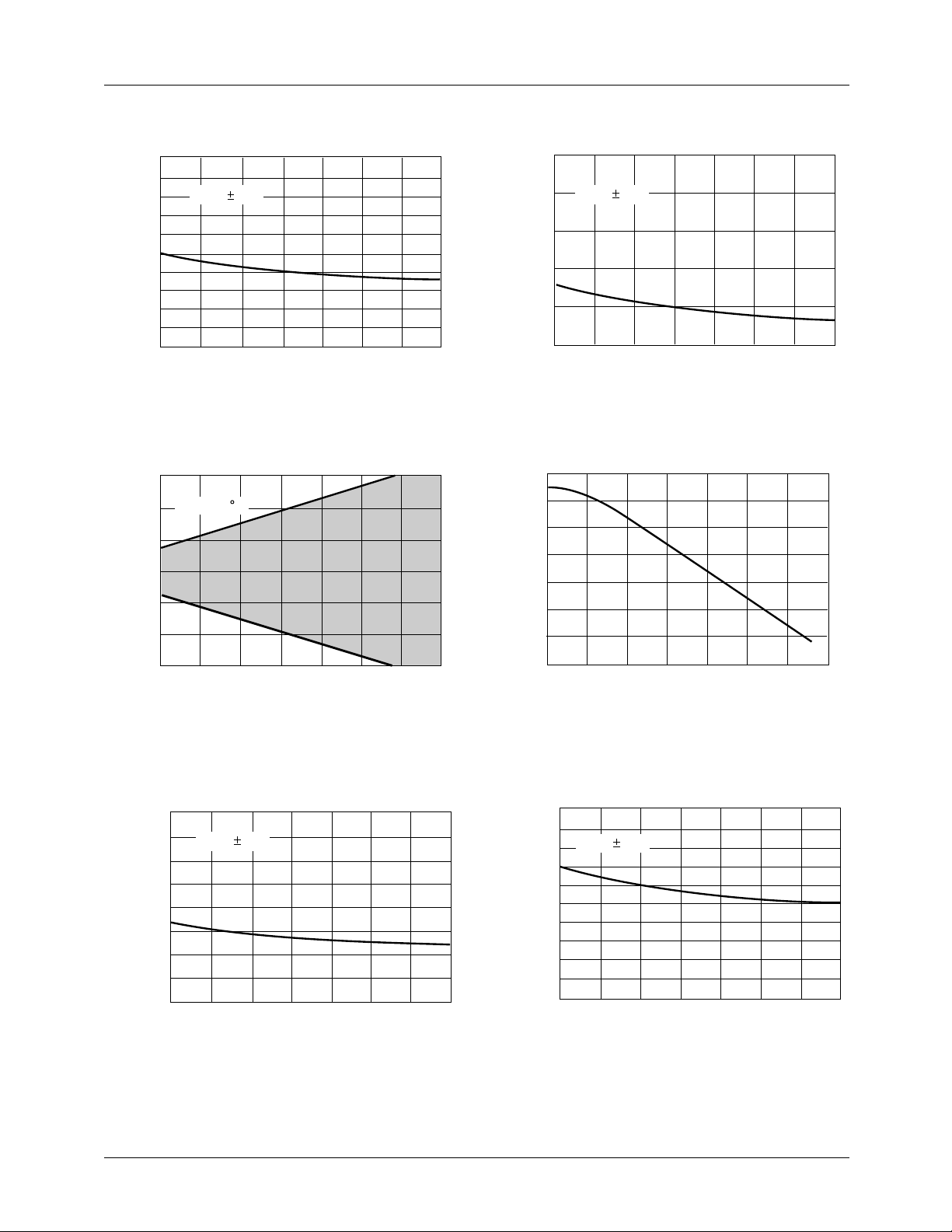
65 0216
0
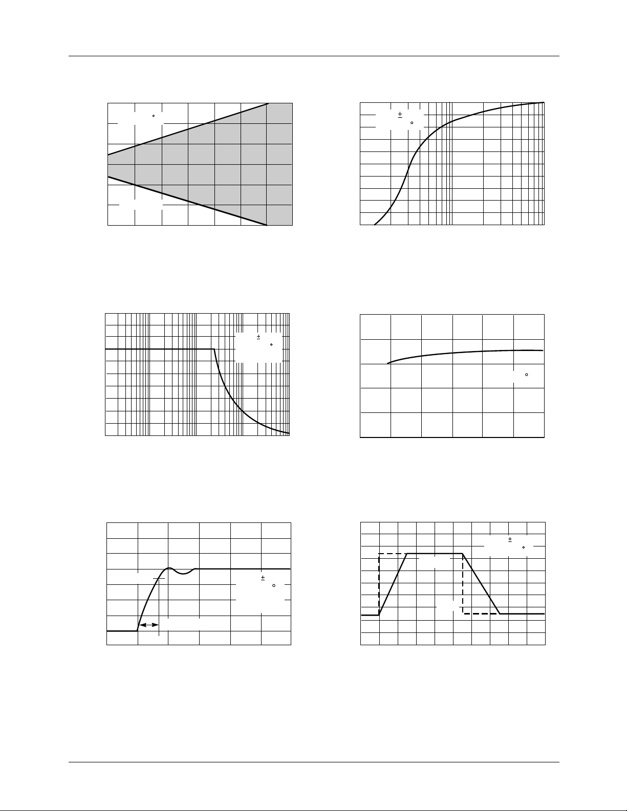
Typical Performance Characteristics
100
80
V = 15V
S
60
(nA)
B
I
40
20
0
0 +10 +20 +30 +40 +50 +60 +70
TA (¡C)
65-0211
25
20
V = 15V
S
15
(nA)
OS
10
I
5
0
0 +10 +20 +30 +40 +50 +60 +70
TA (¡C)
65-0212
Figure 1. Input Bias Current vs. Temperature Figure 2. Input Offset Current vs. Temperature
15
10
T = +25 C
A
5
0
(V)
CM
V
-5
-10
-15
65-0213
±4 ±6 ±8 ±10 ±12 ±14 ±16 ±18
±VS (V)
120
100
80
60
(dB)
40
VOL
A
20
0
-20
1 10 100 1K 10K 100K 1M 10M
F (Hz)
65-0214
Figure 3. Input Common Mode Voltage Range Figure 4. Open Loop Voltage Gain vs. Frequency
vs. Supply Voltage
800K
140
600K
400K
(V/mV)
VOL
A
V = 15V
S
R = 2 k
L
120
100
(mV)
W
C
P
80
V = 15V
S
200K
60
0
0 +10 +20 +30 +40 +50 +60 +70
TA (¡C)
65-0215
0 +10 +20 +30 +40 +50 +60 +7
TA (¡C)
Figure 5. Open Loop Voltage Gain vs. Temperature Figure 6. Power Consumption vs. Temperature
4
RC4558 PRODUCT SPECIFICATION
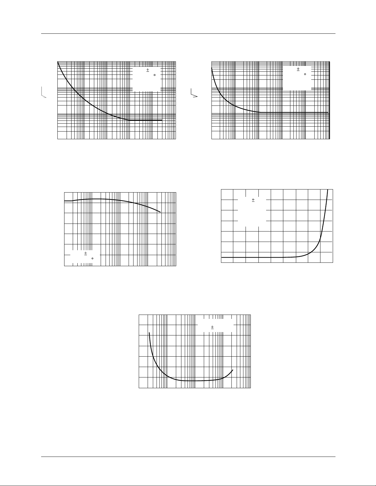
Typical Performance Characteristics (continued)
15
T = +25 C
A
10
5
(V)
0
OUT
V
-5
-10
R = 2 k
W
L
-15
±4 ±6 ±8 ±10 ±12 ±14 ±16 ±18
+VS/-VS (V)
65-0217
28
26
24
V = 15V
S
T = +25 C
A
22
20
(V)
18
16
OUT P-P
V
14
12
10
8
0.1 1.0 10
RL (kW)
Figure 7. Output Voltage Swing vs. Supply Voltage Figure 8. Output Voltage Swing vs. Load Resistance
40
5
36
32
28
24
(V)
20
16
OUT P-P
V
12
8
V = 15V
S
T = +25 C
A
R = 2 kW
L
(mA)
Q
I
4
3
T = +25 C
A
2
1
4
0
100 1K 10K 100K 1M
F (Hz)
65-0219
0
0 ±3 ±6 ±9 ±12 ±15 ±18
+VS/-VS (V)
65-0218
65-0220
Figure 9. Output Voltage Swing vs. Freqeuncy Figure 10. Quiescent Current vs. Supply Voltage
(V)
OUT
V
10
-10
8
6
4
2
Output
V = 15V
S
T = +25 C
A
0
-2
-4
Input
-6
-8
0 10203040
Time (µS)
28
24
20
16
(mV)
12
OUT
V
90%
8
4
0
10% Rise Time
V = 15V
S
T = +25 C
A
R = 2 k
C = 100 pF
W
L
L
65-0221
0 0.25 0.50 0.75 1.00 1.25
Time (µS)
Figure 11. Transient Response Output Figure 12. Follower Large Signal Pulse Response
Voltage vs. Time Output Voltage vs. Time
65-0222
5
PRODUCT SPECIFICATION RC4558
65 0226
Typical Performance Characteristics (continued)
100
V = 15V
S
T = +25 C
A
W
R = 50
10
(pA/ Hz)
0
N
I
S
A = 60 dB
V
0.1
1 10 100 1K 10K 100K
F (Hz)
65-0223
1000
100
(nV/ Hz)
n
10
e
1
0
V = 15V
S
T = +25 C
A
W
R = 50
S
A = 60 dB
V
10 100 1K 10K 100K
F (Hz)
Figure 13. Input Noise Current Density vs. Frequency Figure 14. Input Noise Voltage Density vs. Frequency
140
120
100
80
60
CS (dB)
40
20
0
10
V = 15V
S
T = +25 C
A
100 1K 10K 100K
F (Hz)
65-0225
0.6
0.5
0.4
0.3
THD (%)
0.2
0.1
0
1
V = 15V
S
R = 2K
L
A = 40 dB
V
f = 1 kHz
R = 1k
S
23
W
4
5
V (V )
OUT RMS
678910
65-0224
Figure 15. Channel Separation vs. Frequency Figure 16. Total Harmonic Distortion vs Output Voltage
0.6
OUT
V = 30V
S
RMS
V = 1 V
0.5
0.4
0.3
THD (%)
0.2
0.1
0
10
100 1K 10K 100K
65-0227
F (Hz)
Figure 17. Distortion vs. Frequency
6
RC4558 PRODUCT SPECIFICATION
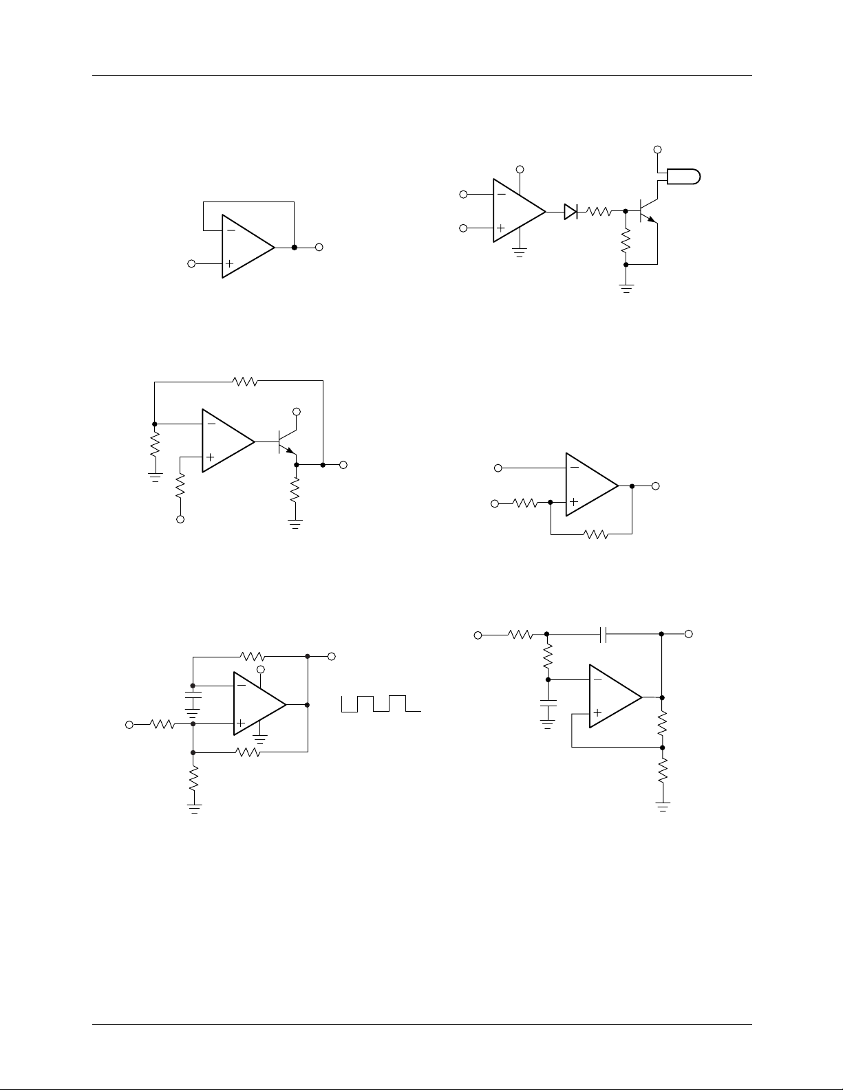
Typical Applications
+V
S
+V
S
100K
2
2
4558A
V
3
IN
1
V
65-0228
OUT
3
4558A
8
1
100
W
4
5K
Figure 18. Voltage Follower Figure 19. Lamp Driver
910K
+V
S
2
4558A
3
91K
A = 10
V
IN
1
2
3
4558A
10M
1
+V
-V
REF
IN
10K
V
OUT
100K
V
65-0230
Figure 20. Power Amplifier Figure 21. Comparator With Hysteresis
65-0229
V
OUT
65-0231
+V
S
16K
0.01µF
2
3
4558A
1
100K
0.001µF
2
3
100K
4558A
V
IN
V
+V
S
1
OUT
1
0
0.01µF
4
16K
100K
100K
100K
65-0232
100K
Figure 22. Squarewave Oscillator Figure 23. DC Coupled 1kHz Low-Pass Active Filter
V
OUT
65-0233
7

PRODUCT SPECIFICATION RC4558
Typical Applications (continued)
V
IN
100K
0.1µF
10µF
1M
+V
2
4558A
3
1M
4
8
4
100K
S
1
100K
10K
+V
V
OUT
S
65-0234
+V
100K
+V
V
IN
S
10K
2
3
4558A
S
1
V
OUT
4
100K
10K
m
100K10 F
65-0236
Figure 24. AC Coupled Non-Inverting Amplifier Figure 25. AC Coupled Inverting Amplifier
V
390K
IN
0.01µF
390K
+V
S
2
39K
620½
0.01 µF
4558A
3
1
4
10µF
620K
100K
120K
6
5
100K
-V
4558B
V
OUT
S
8
7
4
+V
+V
S
65-0235
Figure 26. 1kHz Bandpass Active Filter
0.05 µF
6
5
100K
4558B
7
V
V
OUT 1
OUT 2
100K
C*
51K
R/2
50K
2
3
51K
4558A
51K
1
+V /2
S
10K
* Wide control voltage range: 0V < VS < 2(+VS – 1.5VS)
65-0237
Figure 27. Voltage Controlled Oscillator (VCO)
8
RC4558 PRODUCT SPECIFICATION
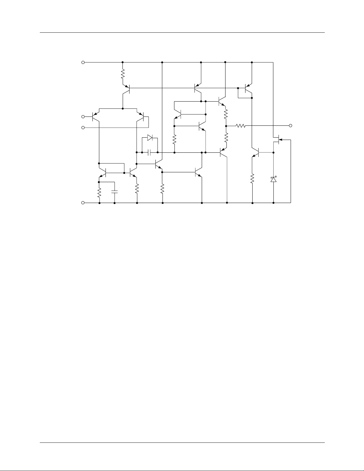
Simplified Schematic Diagram
+V
S
(8)
R1
8.7K
-Input
+Input
-V
(4)
(2,6)
(3,5)
S
Q5
Q2 Q1
Q3
R2
5K
15 pF
C1
Q4
C2
15 pF
R3
5K
D1
Q9
Q13
R4
50K
R5
50K
Q10
Q11
Q12
Q14
Q15
R6
27
R7
27
120
Q8
Q6
5.8K
Output
(1,7)
Q7
D2
65-0208
9

PRODUCT SPECIFICATION RC4558
Ordering Information
Product Number Temperature Range Screening Package
RC4558M 0° to 70°C Commercial 8 Pin Wide SOIC
RC4558N 0° to 70°C Commercial 8 Pin Plastic DIP
RM4558D 0° to 70°C Commercial 8 Pin Ceramic DIP
RM4558D/883B -55°C to +125°C Military 8 Pin Ceramic DIP
Note:
1./883B suffix denotes MIL-STD-883, Par. 1.2.1 compliant device.
LIFE SUPPORT POLICY
FAIRCHILD’S PRODUCTS ARE NOT AUTHORIZED FOR USE AS CRITICAL COMPONENTS IN LIFE SUPPORT DEVICES
OR SYSTEMS WITHOUT THE EXPRESS WRITTEN APPROVAL OF THE PRESIDENT OF FAIRCHILD SEMICONDUCTOR
CORPORATION. As used herein:
1.Life support devices or systems are devices or systems
which, (a) are intended for surgical implant into the body,
or (b) support or sustain life, and (c) whose failure to
perform when properly used in accordance with
instructions for use provided in the labeling, can be
reasonably expected to result in a significant injury of the
user.
2.A critical component in any component of a life support
device or system whose failure to perform can be
reasonably expected to cause the failure of the life support
device or system, or to affect its safety or effectiveness.
www.fairchildsemi.com
5/20/98 0.0m 001
Ó 1998 Fairchild Semiconductor Corporation
Stock#DS30004558
 Loading...