查询RC4391供应商
PRODUCT SPECIFICATION RC4391
2
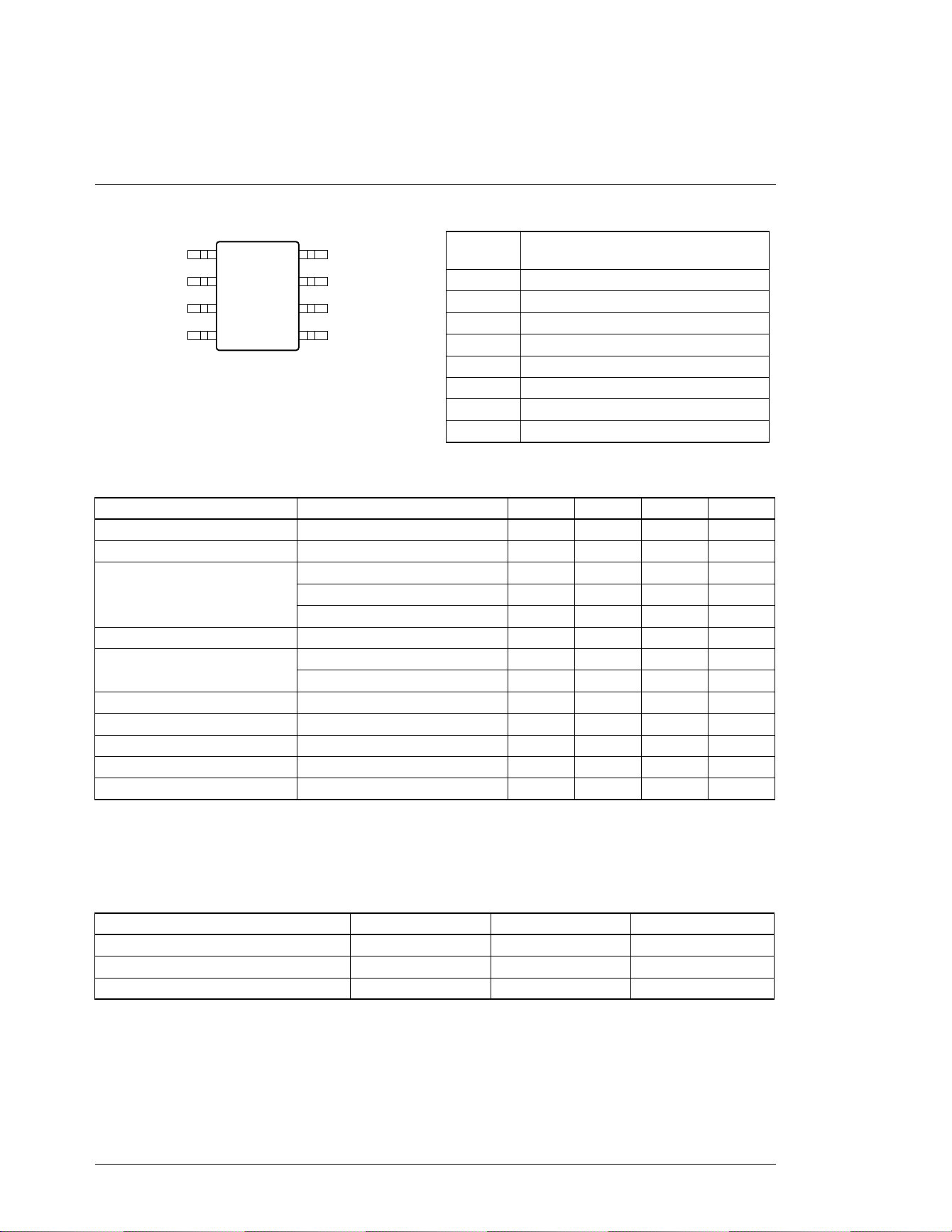
Pin Assignments
LBR
LBD
C
X
GND
V
FB
V
REF
+V
S
L
X
8
65-3471-02
7
6
5
1
2
3
4
Absolute Maximum Ratings
Note:
1. The maximum allowable supply voltage (+V
S
) in inverting applications will be reduced by the value of the negative output
voltage, unless an external power transistor is used in place of Q1.
Thermal Characteristics
Parameter Conditions Min Typ Max Unit
Internal Power Dissipation 500 mW
Supply Voltage
1
(Pin 6 to Pin 4 or Pin 6 to Pin 5) +30 V
Operating Temperature RC4391 0 70 °C
RV4391 -25 85 °C
RM4391 -55 125 °C
Storage Temperature -65 150 °C
Junction Temperature PDIP, SOIC 125 °C
CerDIP 175 °C
Switch Current (I
MAX
) Peak 375 mA
PD TA <50˚C PDIP 468 mW
CerDIP 833 mW
SOIC 300 mW
Lead Soldering Temperature (10 seconds) 300 °C
8-Lead Plastic DIP 8-Lead Ceramic DIP Small Outline SO-8
Therm. Res q
JC
—45°C/W —
Therm. Res. q
JA
160°C/W 150°C/W 240°C/W
For TA >50˚C Derate at 6.25 mW/°C 8.33 mW/°C 4.17 mW/°C
Pin Descriptions
Pin
Number Pin Function Description
1 Low Battery Resistor (LBR)
2 Low Battery Detector (LBD)
3 Timing Capacitor (CX)
4 Ground
5 External Inductor (LX)
6 +Supply Voltage (+VS)
7 +1.25V Reference Voltage (V
REF
)
8 Feedback Voltage (V
FB
)

RC4391 PRODUCT SPECIFICATION
3
Electrical Characteristics
(VS = +6.0V, over the full operating temperature range unless otherwise noted)
Note:
1. The maximum allowable supply voltage (+V
S
) in inverting applications will be reduced by the value of the negative output
voltage, unless an external power transistor is used.
Symbol Parameters Condition Min Typ Max Units
+V
S
Supply Voltage (Note 1) 4.0 30 V
I
SY
Supply Current VS = +25V 300 500 mA
V
REF
Reference Voltage 1.13 1.25 1.36 V
V
OUT
Output Voltage V
OUT nom
= -5.0V -5.5 -5.0 -4.5 V
V
OUT nom
= -15V -16.5 -15.0 -13.5
LI
1
Line Regulation V
OUT nom
= -5.0V, %V
OUT
CX = 150pF
VS = +5.8V to +15V 2.0 4.0
V
OUT nom
= -15V,
CX = 150pF
VS = +5.8V to +15 1.5 3.0
L0
1
Load Regulation V
OUT nom
= -5.0V, %V
OUT
CX = 350pF, VS = +4.5V,
P
LOAD
= 0mW to 75mW 0.2 0.5
V
OUT nom
= -15V,
CX = 350pF, VS = +4.5V,
P
LOAD
= 0mW to 75mW 0.2 0.3
I
CO
Switch Leakage Current Pin 5 = -20V 0.1 30 mA

PRODUCT SPECIFICATION RC4391
4
Electrical Characteristics
(VS = +6.0V, TA = +25°C unless otherwise noted)
Symbol Parameters Condition Min Typ Max Units
I
SY
Supply Voltage VS = +4.0V, 170 250 mA
No External Loads
VS = +25V 300 500
No External Loads
V
OUT
Output Voltage V
OUT nom
= -5.0V -5.35 -5.0 -4.65 V
V
OUT nom
= -15V -15.85 -15.0 -14.15
LI
1
Line Regulation V
OUT nom
= -5.0V %V
OUT
CX = 150pF, 1.5 3.0
VS = +5.8V to +15V
V
OUT nom
= -15V,
CX = 150pF 1.0 2.0
VS = +5.8V to +15V
L0
1
Load Regulation V
OUT nom
= -5.0V, %V
OUT
CX = 350pF, VS = +4.5V, 0.2 0.4
P
LOAD
= 0mW to 75mW
V
OUT nom
= -15V,
CX = 350pF, VS = +4.5V, 0.07 0.14
P
LOAD
= 0mW to 75mW
V
REF
Reference Voltage 1.18 1.25 1.32 V
I
SW
Switch Current Pin 5 = 5.5V 75 100 mA
I
CO
Switch Leakage Current Pin 5 = -24V 0.01 5.0 mA
I
CX
Cap. Charging Current Pin 3 = 0V 6.0 10 14 mA
I
LBDL
LBD Leakage Current Pin 1 = 1.5V, Pin 2 = 6.0V 0.01 5.0 mA
I
LBD0
LBD On Current Pin 1 = 1.1V, Pin 2 = 0.4V 210 600 mA
I
LBRB
LBR Bias Current Pin 1 = 1.5V 0.7 mA
RC4391 PRODUCT SPECIFICATION
5
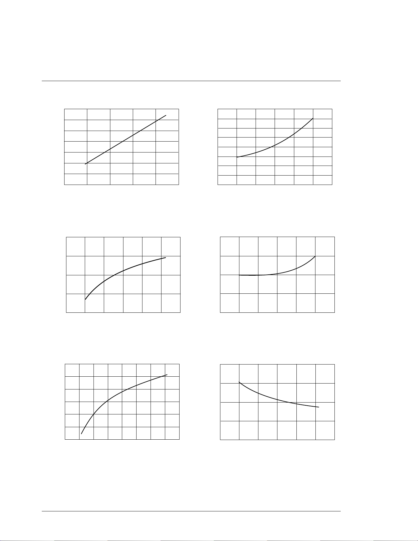
Typical Performance Characteristics
Figure 1. Oscillator Frequency vs. Supply Voltage Figure 2. Oscillator Frequency vs. Temperature
Figure 3. Reference Voltage vs. Temperature Figure 4. Reference Voltage vs. Supply Voltage
Figure 5. Collector Current vs. Q1 Saturation Voltage Figure 6. Minimum Supply Voltage vs. Temperature
F
O
(kHz)
+VS (V)
65-3268
0
510152025
6.5
6.0
5.5
5.0
4.5
4.0
3.5
3.0
F (kHz)
TA (¡C)
65-3272
-55 0 25 70 125
8
7
6
5
4
3
2
1
0
O
V
REF
(V)
TA (¡C)
65-3269
-55 0 25 70 125
1.260
1.255
1.250
1.245
1.240
V
REF
(V)
+VS (V)
65-3273
4 6 10 20 30
1.260
1.255
1.250
1.245
1.240
I
C
(mA)
V
CE
(SAT) (V)
65-3270
600
500
400
300
200
100
0
123 5 7
8
20
10
46
TA (¡C)
65-3271
-55 0 25 70 125
4
3
2
1
0
+V
S
(V)
PRODUCT SPECIFICATION RC4391
6
Principles of Operation
The basic switching inverter circuit is the building block on
which the complete inverting application is based.
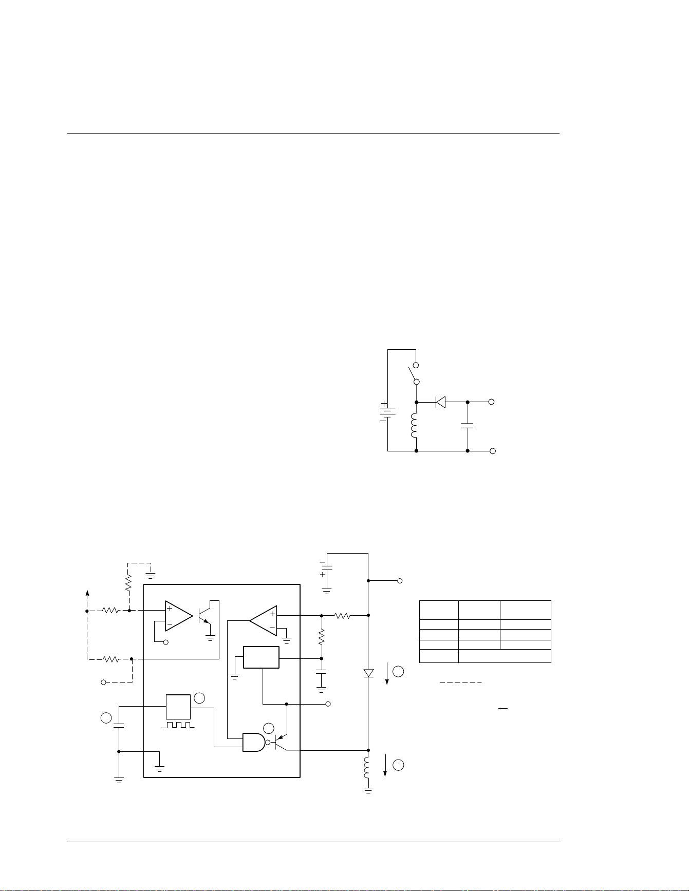
A simplified diagram of the voltage inverter circuit with
ideal components and no feedback circuitry is shown in
Figure 7. When the switch S is closed, charging current from
the battery flows through the inductor L, which builds up a
magnetic field, increasing as the switch is held closed. When
the switch is opened, the magnetic field collapses, and the
energy stored in the magnetic field is conv erted into a current
which flows through the inductor in the same direction as the
changing current. Because there is no path for this current to
flow through the switch, the current must flow through the
diode to charge the capacitor C. The key to the inversion is
the ability of the inductor to become a source when the
charging current is removed.
The equation V = L (di/dt) gives the maximum possible
voltage across the inductor; in the actual application, feedback circuitry and the output capacitor will decrease the
output voltage to a regulated fixed value.
A complete schematic for the standard inverting application
is shown in Figure 8. The ideal switch in the simplified
diagram is replaced by the PNP transistor switch between
pins 5 and 6. C
F
functions as the output filter capacitor, and
D1 and LX replace D and L.
When power is first applied, the ground sensing comparator
(pin 8) compares the output voltage to the +1.25V voltage
reference. Because C
F
is initially discharged a positive
voltage is applied to the comparator, and the output of the
comparator gates the squarewave oscillator. This gated
squarewave signal turns on, then off, the PNP output transistor. This turning on and off of the output transistor performs
the same function as opening and closing the ideal switch in
the simplified diagram; i.e., it stores energy in the inductor
during the on time and releases it into the capacitor during
the off time.
The comparator will continue to allow the oscillator to turn
the switch transistor on and off until enough energy has been
stored in the output capacitor to make the comparator input
voltage decrease to less than 0V. The voltage applied to the
comparator is set by the output voltage, the reference voltage, and the ratio of R1 to R2.
Figure 7. Simple Inverting Regulator
D
(+)
(–)
V
OUT
C
S
L
+V
S
65-1601
*Caution: Use current limiting protection circuit for high values of CF (Figure 13)
Figure 8. Inverting Regulator – Standard Circuit
C2
C1
OSC
+1.25V
REF/Bias
RC4391
65-1602
REF
V
Q1
Q2
C
x
A
To
+V
s
LBD
Output
R3
260K
R4
590K
R6
100K
B
C *
33µF
F
R1
R2
+V
s
V
OUT
1N914
F
E
L
x
C1
0.1µF
D1
-
Parts
List
-5.0V
Output
-15V
Output
R1 =
R2 =
C =
L =
300 k
75 k
150 pF
1.0 mH Dale TE3 Q4 TA
900 k
75 k
150 pF
= Optional
-V = (1.25V) ( )
x
x
W
W
W
W
OUT
R1
R2
D
LBR
GND
C
X
LBD
L
X
+V
S
V
REF
V
FB
RC4391 PRODUCT SPECIFICATION
7
Figure 9. Inverting Regulator Waveforms
B
A
C
D
E
F
G
1.78V
0.62V
(Internal)
I
0 mA
+V
(Internal)
+V - 0.7V
Max
0 mA
I
0 mA
+V - V
-V - V
Ground
C
O
I
V
I
I
V
X
SC
LOAD
BEQ1
LX
D
LX
L
S
S
S
MAX
SW
OUT D
65-2472
BAT
OUT
X
X
V
L
V
L
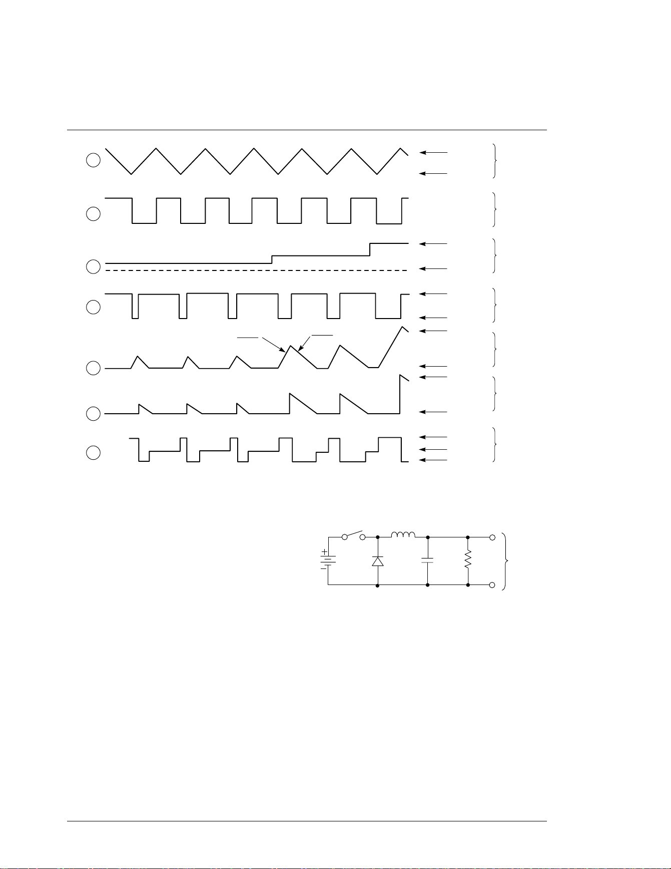
This feedback system will vary the duration of the on time in
response to changes in load current or battery voltage (see
Figure 9). If the load current increases (waveform C), then
the transistor will remain on (waveform D) for a longer portion of the oscillator cycle, (waveform B) to build up to a
higher peak value. The duty cycle of the switch transistor
varies in response to changes in load and line.
Step-Down Regulator
The step-down circuit function is similar to inv ersion; it uses
the same components (switch, inductor, diode, filter capacitor), and charges and discharges the inductor by closing and
opening the switch. The great difference is that the inductor
is in series with the load; therefore, both the charging current
and the discharge current flow into the load. In the inverting
circuit only the discharge current flows into the load. Refer
to Figure 10.
When the switch S is closed, current flows from the battery,
through the inductor, and through the load resistor to ground.
After the switch is opened, stored energy in the inductor
causes current to keep flowing through the load, the circuit
being completed by the catch diode D. Since current flows to
the load during charge and discharge, the average load cur-
rent will be greater than in an inverting circuit. The significance of that is that for equal load currents the step-down
circuit will require less peak inductor current than an inverting circuit. Therefore, the inductor will not require as large
of a core, and the switch transistor will not be stressed as
heavily for equal load currents.
Figure 11 depicts a complete schematic for a step-down circuit using the RC4391. Observe that the ground lead of the
4391 is not connected to circuit ground; instead, it is tied to
the output voltage. It is by this rearrangement that the feedback system, which senses voltages more negative than the
ground lead, can be used to regulate a non-negative output
voltage.
Figure 10. Simple Step-Down Regulator
D
(+)
(-)
V
OUT
S
C
S
L
+V
65-2473
R
L
 Loading...